Может есть смысл переработать проект и сделать как сделал K3NG в контроллере поворотки?
У него весь проект разбит на отдельные функции (хидеры) и эти функции выведены в отдельные файлы.
Может есть смысл переработать проект и сделать как сделал K3NG в контроллере поворотки?
У него весь проект разбит на отдельные функции (хидеры) и эти функции выведены в отдельные файлы.
если знаешь, что кусок кода менялся в конкретном файле то наверное всё же проще
такой механизм стыкуется с git
к примеру - tester_setup.h, tester_features.h, tester_hardware.h, tester_pins.h, tester_display.h и основной скетч )))
в начале файла в комментах указываем, откуда и что попадает
да и листинги будут тогда удобоваримыми, как мне кажется...
в молодости я тоже тысячи строк держал в уме, сейчас - УВЫ )))
если знаешь, что кусок кода менялся в конкретном файле то наверное всё же проще
такой механизм стыкуется с git
к примеру - tester_setup.h, tester_features.h, tester_hardware.h, tester_pins.h, tester_display.h и основной скетч
в начале файла в комментах указываем, откуда и что попадает
И что мешает самому преобразовать код разработчиков в рабочий скетч для Ардуино?
Отсутствие какого-нибудь опыта в этом, на СИ программ не писал, только ассемблер и в машинных кодах, да и по процессорам интел и моторола, честно сказать попытался, с ходу не получилось ))) все свои программы были написаны до 1990 года однако )))
Но "религия ардуино" мне понравилась, эти бы возможности лет бы так тридцать, сорок назад )))
Странная ситуёвина, на работе компилировал под версией 1.6.5 и компилировалось без ошибок
(под дисплей I2C), под версией 1.6.8 и 1.6.12 не пошло, это да )))
Сейчас второй час дома пытаюсь скомпилировать и эффект нулевой (собрал девайс на макетке пытаюсь залить), видимо всё дело в библиотеке под I2C, с этой же библиотекой контроллер K3NG и компилируется и заливается без проблем ))) чудеса с этими ардуинками, IDE девственно чистый, даже перекачал заново, а не сбросите свою библиотеку по I2C?
Кстати, правильная строка инициализации для моей библиотеки LCD_I2C (и моего дисплея)
В продолжении темы - притащил с работы всё в конфигурации где компилируется, выполняю, заливаю, не "выходит каменный цветок"
Вот это реально отпугивает... кто готов помочь?
да это понятно - я про инициализационную строку lcd
Библиотека заработала, но эту строку поправил - #define lcd_init() lcd.begin(16,2)
Поменял на lcd.begin()
Под 1.6.5 не компилил из-за этого
На дисплее что-то есть, всё на макетке, нет конденсатора на aref и кнопку еще не ставил, но уже что-то там тестит, какие-то транзисторы находит )))
а вот версия 1.08.2 скомпилилась, ничего править не пришлось, макетирую на UNO, наверное я что-то напутал в схеме - несёт пургу ))), если что-то к измерительным выводам присоеденено на момент включения - встряёт, кнопка не работает
Но самое главное - ожил )))
Пошевелил проводки, попередёргивал и, как-то неожиданно заработало )))
Резисторы меряет вполне точно, а вот электролиты врёт, завышает более чем в два раза.
А как ввести ИОН в схему?
ARDUINEC - а Вы это в своём устройстве задействовали?
// Port pin for 2.5V precision reference used for VCC check (optional)
#define TPREF 4
// Port pin for Battery voltage measuring
#define TPBAT 5
А то точность процентов 5-10 на резисторах у меня на UNO получилась, резисторы в прибор специально не отбирал )))
Всё таки дисплейчики надо бы выделить как-то в отдельный класс...
Правлю для дисплея 2004 под I2С, код по всему скетчу разбросан, как-то несиматишна )))
Понимаю, это будет уже совсем другой проект по сравнению с авторским от разработчика тестера
ЗЫ дисплей работает но есть мешанина, я о LCD2004, правлю
/* \\\|///
\\ - - //
( @ @ )
/--------------------oOOo-(_)-oOOo---------------------\
| |
| |
| Transistor Tester for Arduino (version 1.08a) |
| |
| based on code: Karl-Heinz Kubbeler (version 1.08k) |
| |
| |
| Oooo |
\--------------------oooO----( )---------------------/
( ) ) /
\ ( (_/
\_) */
#include <avr/io.h>
#include <util/delay.h>
#include <avr/sleep.h>
#include <stdlib.h>
#include <string.h>
#include <avr/eeprom.h>
#include <avr/pgmspace.h>
#include <avr/wdt.h>
#include <avr/interrupt.h>
#include <math.h>
#include <stdint.h>
#include <avr/power.h>
#define LCD1602
//#define LCD2004
#define LCD_I2C
//#define NOK5110
#ifdef LCD2004
#ifdef LCD_I2C
#include <Wire.h>
#include <LiquidCrystal_I2C.h>
#else
#include <LiquidCrystal.h>
#endif
#endif
#ifdef LCD1602
#ifdef LCD_I2C
#include <Wire.h>
#include <LiquidCrystal_I2C.h>
#else
#include <LiquidCrystal.h>
#endif
#endif
#ifdef NOK5110
#include <SPI.h>
#include <Adafruit_GFX.h>
#include <Adafruit_PCD8544.h>
#endif
// ******** config options for your Semiconductor tester
// Every changing of this Makefile will result in new compiling the whole
// programs, if you call make or make upload.
#define MCU atmega328p
#define F_CPU 16000000UL
// Select your language:
// Available languages are: LANG_ENGLISH, LANG_GERMAN, LANG_POLISH, LANG_CZECH, LANG_SLOVAK, LANG_SLOVENE,
// LANG_DUTCH, LANG_BRASIL, LANG_RUSSIAN, LANG_UKRAINIAN
#define LANG_ENGLISH
// The LCD_CYRILLIC option is necessary, if you have a display with cyrillic characterset.
// This lcd-display don't have a character for Ohm and for u (micro).
// Russian language requires a LCD controller with russian characterset and option LCD_CYRILLIC!
#define LCD_CYRILLIC
// The LCD_DOGM option must be set for support of the DOG-M type of LCD modules with ST7036 controller.
// For this LCD type the contrast must be set with software command.
//#define LCD_DOGM
// Option STRIP_GRID_BOARD selects different board-layout, do not set for standard board!
// The connection of LCD is totally different for both versions.
//#define STRIP_GRID_BOARD
// The WITH_SELFTEST option enables selftest function (only for mega168 or mega328).
//#define WITH_SELFTEST
// AUTO_CAL will enable the autocalibration of zero offset of capacity measurement and
// also the port output resistance values will be find out in SELFTEST section.
// With a external capacitor a additionally correction of reference voltage is figured out for
// low capacity measurement and also for the AUTOSCALE_ADC measurement.
// The AUTO_CAL option is only selectable for mega168 and mega328.
//#define AUTO_CAL
// FREQUENCY_50HZ enables a 50 Hz frequency generator for up to one minute at the end of selftests.
//#define FREQUENCY_50HZ
// The WITH_AUTO_REF option enables reading of internal REF-voltage to get factors for the Capacity measuring.
#define WITH_AUTO_REF
// REF_C_KORR corrects the reference Voltage for capacity measurement (<40uF) and has mV units.
// Greater values gives lower capacity results.
#define REF_C_KORR 12
// REF_L_KORR corrects the reference Voltage for inductance measurement and has mV units.
#define REF_L_KORR 40
// C_H_KORR defines a correction of 0.1% units for big capacitor measurement.
// Positive values will reduce measurement results.
#define C_H_KORR 0
// The WITH_UART option enables the software UART (TTL level output at Pin PC3, 26).
// If the option is deselected, PC3 can be used as external voltage input with a
// 10:1 resistor divider.
//#define WITH_UART
// The CAP_EMPTY_LEVEL defines the empty voltage level for capacitors in mV.
// Choose a higher value, if your Tester reports "Cell!" by unloading capacitors.
#define CAP_EMPTY_LEVEL 4
// The AUTOSCALE_ADC option enables the autoscale ADC (ADC use VCC and Bandgap Ref).
#define AUTOSCALE_ADC
#define REF_R_KORR 3
// The ESR_ZERO value define the zero value of ESR measurement (units = 0.01 Ohm).
//#define ESR_ZERO 29
#define ESR_ZERO 20
// NO_AREF_CAP tells your Software, that you have no Capacitor installed at pin AREF (21).
// This enables a shorter wait-time for AUTOSCALE_ADC function.
// A capacitor with 1nF can be used with the option NO_AREF_CAP set.
#define NO_AREF_CAP
// The OP_MHZ option tells the software the Operating Frequency of your ATmega.
// OP_MHZ 16
// Restart from sleep mode will be delayed for 16384 clock tics with crystal mode.
// Operation with the internal RC-Generator or external clock will delay the restart by only 6 clock tics.
// You must specify this with "#define RESTART_DELAY_TICS=6", if you don't use the crystal mode.
//#define RESTART_DELAY_TICS 6
// The USE_EEPROM option specify where you wish to locate fix text and tables.
// If USE_EEPROM is unset, program memory (flash) is taken for fix text and tables.
//#define USE_EEPROM
// Setting EBC_STYPE will select the old style to present the order of Transistor connection (EBC=...).
// Omitting the option will select the 123=... style. Every point is replaced by a character identifying
// type of connected transistor pin (B=Base, E=Emitter, C=Collector, G=Gate, S=Source, D=Drain).
// If you select EBC_STYLE=321 , the style will be 321=... , the inverted order to the 123=... style.
//#define EBC_STYLE
//#define EBC_STYLE 321
// Setting of NO_NANO avoids the use of n as prefix for Farad (nF), the mikro prefix is used insted (uF).
//#define NO_NANO
// The PULLUP_DISABLE option disable the pull-up Resistors of IO-Ports.
// To use this option a external pull-up Resistor (10k to 30k)
// from Pin 13 to VCC must be installed!
#define PULLUP_DISABLE
// The ANZ_MESS option specifies, how often an ADC value is read and accumulated.
// Possible values of ANZ_MESS are 5 to 200.
#define ANZ_MESS 25
// The POWER_OFF option enables the power off function, otherwise loop measurements infinitely
// until power is disconnected with a ON/OFF switch (#define POWER_OFF).
// If you have the tester without the power off transistors, you can deselect POWER_OFF .
// If you have NOT selected the POWER_OFF option with the transistors installed,
// you can stop measuring by holding the key several seconds after a result is
// displayed. After releasing the key, the tester will be shut off by timeout.
// Otherwise you can also specify, after how many measurements without found part
// the tester will shut down (#define POWER_OFF=5).
// The tester will also shut down with found part,
// but successfull measurements are allowed double of the specified number.
// You can specify up to 255 empty measurements (#define POWER_OFF=255).
//#define POWER_OFF 5
//#define POWER_OFF
// Option BAT_CHECK enables the Battery Voltage Check, otherwise the SW Version is displayed instead of Bat.
// BAT_CHECK should be set for battery powered tester version.
//#define BAT_CHECK
// The BAT_OUT option enables Battery Voltage Output on LCD (if BAT_CHECK is selected).
// If your 9V supply has a diode installed, use the BAT_OUT=600 form to specify the
// threshold voltage of your diode to adjust the output value.
// This threshold level is added to LCD-output and does not affect the voltage checking levels.
//#define BAT_OUT 150
// To adjust the warning-level and poor-level of battery check to the capability of a
// low drop voltage regulator, you can specify the Option BAT_POOR=5400 .
// The unit for this option value is 1mV , 5400 means a poor level of 5.4V.
// The warning level is 0.8V higher than the specified poor level (>5.3V).
// The warning level is 0.4V higher than the specified poor level (>2.9V, <=5.3V).
// The warning level is 0.2V higher than the specified poor level (>1.3V, <=2.9V).
// The warning level is 0.1V higher than the specified poor level (<=1.3V).
// Setting the poor level to low values is not recommended for rechargeable Batteries,
// because this increase the danger for deep discharge!!
#define BAT_POOR 6400
// The sleep mode of the ATmega168 or ATmega328 is normally used by the software to save current.
// You can inhibit this with the option INHIBIT_SLEEP_MODE .
//#define INHIBIT_SLEEP_MODE
// ******** end of selectable options
/* -=- -=- -=- -=- -=- -=- -=- -=- -=- -=- -=- -=- -=- -=- -=- -=- -=- -=- -=- -=- -=- -=- -=- -=- -=- -=- -=- -=- */
// ######## Configuration
#ifndef ADC_PORT
//#define DebugOut 3 // if set, output of voltages of resistor measurements in row 2,3,4
//#define DebugOut 4 // if set, output of voltages of Diode measurement in row 3+4
//#define DebugOut 5 // if set, output of Transistor checks in row 2+3
//#define DebugOut 10 // if set, output of capacity measurements (ReadCapacity) in row 3+4
/*
Port, that is directly connected to the probes.
This Port must have an ADC-Input (ATmega8: PORTC).
The lower pins of this Port must be used for measurements.
Please don't change the definitions of TP1, TP2 and TP3!
The TPREF pin can be connected with a 2.5V precision voltage reference
The TPext can be used with a 10:1 resistor divider as external voltage probe up to 50V
*/
#define ADC_PORT PORTC
#define ADC_DDR DDRC
#define ADC_PIN PINC
#define TP1 0
#define TP2 1
#define TP3 2
#define TPext 3
// Port pin for 2.5V precision reference used for VCC check (optional)
#define TPREF 4
// Port pin for Battery voltage measuring
#define TPBAT 5
/*
exact values of used resistors (Ohm).
The standard value for R_L is 680 Ohm, for R_H 470kOhm.
To calibrate your tester the resistor-values can be adjusted:
*/
#define R_L_VAL 6800 // standard value 680 Ohm, multiplied by 10 for 0.1 Ohm resolution
//#define R_L_VAL 6690 // this will be define a 669 Ohm
#define R_H_VAL 47000 // standard value 470000 Ohm, multiplied by 10, divided by 100
//#define R_H_VAL 47900 // this will be define a 479000 Ohm, divided by 100
#define R_DDR DDRB
#define R_PORT PORTB
/*
Port for the Test resistors
The Resistors must be connected to the lower 6 Pins of the Port in following sequence:
RLx = 680R-resistor for Test-Pin x
RHx = 470k-resistor for Test-Pin x
RL1 an Pin 0
RH1 an Pin 1
RL2 an Pin 2
RH2 an Pin 3
RL3 an Pin 4
RH3 an Pin 5
*/
#define ON_DDR DDRD
#define ON_PORT PORTD
#define ON_PIN_REG PIND
#define ON_PIN 18 // Pin, must be switched to high to switch power on
#ifdef STRIP_GRID_BOARD
// Strip Grid board version
#define RST_PIN 0 // Pin, is switched to low, if push button is pressed
#else
// normal layout version
#define RST_PIN 17 // Pin, is switched to low, if push button is pressed
#endif
// Port(s) / Pins for LCD
#ifdef STRIP_GRID_BOARD
// special Layout for strip grid board
#define HW_LCD_EN_PORT PORTD
#define HW_LCD_EN_PIN 5
#define HW_LCD_RS_PORT PORTD
#define HW_LCD_RS_PIN 7
#define HW_LCD_B4_PORT PORTD
#define HW_LCD_B4_PIN 4
#define HW_LCD_B5_PORT PORTD
#define HW_LCD_B5_PIN 3
#define HW_LCD_B6_PORT PORTD
#define HW_LCD_B6_PIN 2
#define HW_LCD_B7_PORT PORTD
#define HW_LCD_B7_PIN 1
#else
// normal Layout
#define HW_LCD_EN_PORT PORTD
#define HW_LCD_EN_PIN 6
#define HW_LCD_RS_PORT PORTD
#define HW_LCD_RS_PIN 7
#define HW_LCD_B4_PORT PORTD
#define HW_LCD_B4_PIN 5
#define HW_LCD_B5_PORT PORTD
#define HW_LCD_B5_PIN 4
#define HW_LCD_B6_PORT PORTD
#define HW_LCD_B6_PIN 3
#define HW_LCD_B7_PORT PORTD
#define HW_LCD_B7_PIN 2
#endif
// U_VCC defines the VCC Voltage of the ATmega in mV units
#define U_VCC 5000
// integer factors are used to change the ADC-value to mV resolution in ReadADC !
// With the option NO_CAP_HOLD_TIME you specify, that capacitor loaded with 680 Ohm resistor will not
// be tested to hold the voltage same time as load time.
// Otherwise (without this option) the voltage drop during load time is compensated to avoid displaying
// too much capacity for capacitors with internal parallel resistance.
// #define NO_CAP_HOLD_TIME
// U_SCALE can be set to 4 for better resolution of ReadADC function for resistor measurement
#define U_SCALE 4
// R_ANZ_MESS can be set to a higher number of measurements (up to 200) for resistor measurement
#define R_ANZ_MESS 190
// Watchdog
//#define WDT_enabled
/*
If you remove the "#define WDT_enabled" , the Watchdog will not be activated.
This is only for Test or debugging usefull.
For normal operation please activate the Watchdog !
*/
// ######## End of configuration
#if R_ANZ_MESS < ANZ_MESS
#undef R_ANZ_MESS
#define R_ANZ_MESS ANZ_MESS
#endif
#if U_SCALE < 0
// limit U_SCALE
#undef U_SCALE
#define U_SCALE 1
#endif
#if U_SCALE > 4
// limit U_SCALE
#undef U_SCALE
#define U_SCALE 4
#endif
#ifndef REF_L_KORR
#define REF_L_KORR 50
#endif
// the following definitions specify where to load external data from: EEprom or flash
#ifdef USE_EEPROM
#define MEM_TEXT EEMEM
#if E2END > 0X1FF
#define MEM2_TEXT EEMEM
#define MEM2_read_byte(a) eeprom_read_byte(a)
#define MEM2_read_word(a) eeprom_read_word(a)
#define lcd_fix2_string(a) lcd_fix_string(a)
#else
#define MEM2_TEXT PROGMEM
#define MEM2_read_byte(a) pgm_read_byte(a)
#define MEM2_read_word(a) pgm_read_word(a)
#define lcd_fix2_string(a) lcd_pgm_string(a)
#define use_lcd_pgm
#endif
#define MEM_read_word(a) eeprom_read_word(a)
#define MEM_read_byte(a) eeprom_read_byte(a)
#else
#define MEM_TEXT PROGMEM
#define MEM2_TEXT PROGMEM
#define MEM_read_word(a) pgm_read_word(a)
#define MEM_read_byte(a) pgm_read_byte(a)
#define MEM2_read_byte(a) pgm_read_byte(a)
#define MEM2_read_word(a) pgm_read_word(a)
#define lcd_fix2_string(a) lcd_pgm_string(a)
#define use_lcd_pgm
#endif
// RH_OFFSET : systematic offset of resistor measurement with RH (470k)
// resolution is 0.1 Ohm, 3500 defines a offset of 350 Ohm
#define RH_OFFSET 3500
// TP2_CAP_OFFSET is a additionally offset for TP2 capacity measurements in pF units
#define TP2_CAP_OFFSET 2
// CABLE_CAP defines the capacity (pF) of 12cm cable with clip at the terminal pins
#define CABLE_CAP 3
// select the right Processor Typ
/*
#if defined(__AVR_ATmega48__)
#define PROCESSOR_TYP 168
#elif defined(__AVR_ATmega48P__)
#define PROCESSOR_TYP 168
#elif defined(__AVR_ATmega88__)
#define PROCESSOR_TYP 168
#elif defined(__AVR_ATmega88P__)
#define PROCESSOR_TYP 168
#elif defined(__AVR_ATmega168__)
#define PROCESSOR_TYP 168
#elif defined(__AVR_ATmega168P__)
#define PROCESSOR_TYP 168
#elif defined(__AVR_ATmega328__)
#define PROCESSOR_TYP 328
#elif defined(__AVR_ATmega328P__)
#define PROCESSOR_TYP 328
#elif defined(__AVR_ATmega640__)
#define PROCESSOR_TYP 1280
#elif defined(__AVR_ATmega1280__)
#define PROCESSOR_TYP 1280
#elif defined(__AVR_ATmega2560__)
#define PROCESSOR_TYP 1280
#else
#define PROCESSOR_TYP 8
#endif
*/
#define PROCESSOR_TYP 328
// automatic selection of right call type
#if FLASHEND > 0X1FFF
#define ACALL call
#else
#define ACALL rcall
#endif
// automatic selection of option and parameters for different AVRs
//------------------=========----------
#if PROCESSOR_TYP == 168
//------------------=========----------
#define MCU_STATUS_REG MCUCR
#define ADC_COMP_CONTROL ADCSRB
#define TI1_INT_FLAGS TIFR1
#define DEFAULT_BAND_GAP 1070
#define DEFAULT_RH_FAKT 884 // mega328 1070 mV
// LONG_HFE activates computation of current amplification factor with long variables
#define LONG_HFE
// COMMON_COLLECTOR activates measurement of current amplification factor in common collector circuit (Emitter follower)
#define COMMON_COLLECTOR
#define MEGA168A 17
#define MEGA168PA 18
// Pin resistor values of ATmega168
//#define PIN_RM 196
//#define PIN_RP 225
#define PIN_RM 190
#define PIN_RP 220
// CC0 defines the capacity of empty terminal pins 1 & 3 without cable
#define CC0 36
// Slew rate correction val += COMP_SLEW1 / (val + COMP_SLEW2)
#define COMP_SLEW1 4000
#define COMP_SLEW2 220
#define C_NULL CC0+CABLE_CAP+(COMP_SLEW1 / (CC0 + CABLE_CAP + COMP_SLEW2))
#define MUX_INT_REF 0x0e // channel number of internal 1.1 V
//------------------=========----------
#elif PROCESSOR_TYP == 328
//------------------=========----------
#define MCU_STATUS_REG MCUCR
#define ADC_COMP_CONTROL ADCSRB
#define TI1_INT_FLAGS TIFR1
#define DEFAULT_BAND_GAP 1070
#define DEFAULT_RH_FAKT 884 // mega328 1070 mV
// LONG_HFE activates computation of current amplification factor with long variables
#define LONG_HFE
// COMMON_COLLECTOR activates measurement of current amplification factor in common collector circuit (Emitter follower)
#define COMMON_COLLECTOR
#define PIN_RM 200
#define PIN_RP 220
// CC0 defines the capacity of empty terminal pins 1 & 3 without cable
#define CC0 36
// Slew rate correction val += COMP_SLEW1 / (val + COMP_SLEW2)
#define COMP_SLEW1 4000
#define COMP_SLEW2 180
#define C_NULL CC0+CABLE_CAP+(COMP_SLEW1 / (CC0 + CABLE_CAP + COMP_SLEW2))
#define MUX_INT_REF 0x0e // channel number of internal 1.1 V
//------------------=========----------
#elif PROCESSOR_TYP == 1280
//------------------=========----------
#define MCU_STATUS_REG MCUCR
#define ADC_COMP_CONTROL ADCSRB
#define TI1_INT_FLAGS TIFR1
#define DEFAULT_BAND_GAP 1070
#define DEFAULT_RH_FAKT 884 // mega328 1070 mV
// LONG_HFE activates computation of current amplification factor with long variables
#define LONG_HFE
// COMMON_COLLECTOR activates measurement of current amplification factor in common collector circuit (Emitter follower)
#define COMMON_COLLECTOR
#define PIN_RM 200
#define PIN_RP 220
// CC0 defines the capacity of empty terminal pins 1 & 3 without cable
#define CC0 36
// Slew rate correction val += COMP_SLEW1 / (val + COMP_SLEW2)
#define COMP_SLEW1 4000
#define COMP_SLEW2 180
#define C_NULL CC0+CABLE_CAP+(COMP_SLEW1 / (CC0 + CABLE_CAP + COMP_SLEW2))
#define MUX_INT_REF 0x1e /* channel number of internal 1.1 V */
//------------------=========----------
#else
// ATmega8
//------------------=========----------
#define MCU_STATUS_REG MCUCSR
#define ADC_COMP_CONTROL SFIOR
#define TI1_INT_FLAGS TIFR
#define DEFAULT_BAND_GAP 1298 //mega8 1298 mV
#define DEFAULT_RH_FAKT 740 // mega8 1250 mV
// LONG_HFE activates computation of current amplification factor with long variables
#define LONG_HFE
// COMMON_COLLECTOR activates measurement of current amplification factor in common collector circuit (Emitter follower)
#define COMMON_COLLECTOR
#define PIN_RM 196
#define PIN_RP 240
// CC0 defines the capacity of empty terminal pins 1 & 3 without cable
#define CC0 27
// Slew rate correction val += COMP_SLEW1 / (val + COMP_SLEW2)
#define COMP_SLEW1 0
#define COMP_SLEW2 33
#define C_NULL CC0+CABLE_CAP+(COMP_SLEW1 / (CC0 + CABLE_CAP + COMP_SLEW2))
#define MUX_INT_REF 0x0e /* channel number of internal 1.1 V */
#ifndef INHIBIT_SLEEP_MODE
#define INHIBIT_SLEEP_MODE /* do not use the sleep mode of ATmega */
#endif
#endif
#if PROCESSOR_TYP == 8
// 2.54V reference voltage + correction (fix for ATmega8)
#ifdef AUTO_CAL
#define ADC_internal_reference (2560 + (int8_t)eeprom_read_byte((uint8_t *)&RefDiff))
#else
#define ADC_internal_reference (2560 + REF_R_KORR)
#endif
#else
// all other processors use a 1.1V reference
#ifdef AUTO_CAL
#define ADC_internal_reference (ref_mv + (int8_t)eeprom_read_byte((uint8_t *)&RefDiff))
#else
#define ADC_internal_reference (ref_mv + REF_R_KORR)
#endif
#endif
#ifndef REF_R_KORR
#define REF_R_KORR 0
#endif
#ifndef REF_C_KORR
#define REF_C_KORR 0
#endif
#define LONG_WAIT_TIME 28000
#define SHORT_WAIT_TIME 5000
#ifdef POWER_OFF
// if POWER OFF function is selected, wait 14s
// if POWER_OFF with parameter > 2, wait only 5s before repeating
#if (POWER_OFF+0) > 2
#define OFF_WAIT_TIME SHORT_WAIT_TIME
#else
#define OFF_WAIT_TIME LONG_WAIT_TIME
#endif
#else
// if POWER OFF function is not selected, wait 14s before repeat measurement
#define OFF_WAIT_TIME LONG_WAIT_TIME
#endif
//**********************************************************
// defines for the selection of a correctly ADC-Clock
// will match for 1MHz, 2MHz, 4MHz, 8MHz and 16MHz
// ADC-Clock can be 125000 or 250000
// 250 kHz is out of the full accuracy specification!
// clock divider is 4, when CPU_Clock==1MHz and ADC_Clock==250kHz
// clock divider is 128, when CPU_Clock==16MHz and ADC_Clock==125kHz
#define F_ADC 125000
//#define F_ADC 250000
#if F_CPU/F_ADC == 2
#define AUTO_CLOCK_DIV (1<<ADPS0)
#endif
#if F_CPU/F_ADC == 4
#define AUTO_CLOCK_DIV (1<<ADPS1)
#endif
#if F_CPU/F_ADC == 8
#define AUTO_CLOCK_DIV (1<<ADPS1) | (1<<ADPS0)
#endif
#if F_CPU/F_ADC == 16
#define AUTO_CLOCK_DIV (1<<ADPS2)
#endif
#if F_CPU/F_ADC == 32
#define AUTO_CLOCK_DIV (1<<ADPS2) | (1<<ADPS0)
#endif
#if F_CPU/F_ADC == 64
#define AUTO_CLOCK_DIV (1<<ADPS2) | (1<<ADPS1)
#endif
#if F_CPU/F_ADC == 128
#define AUTO_CLOCK_DIV (1<<ADPS2) | (1<<ADPS1) | (1<<ADPS0)
#endif
//**********************************************************
#define F_ADC_F 500000
#if F_CPU/F_ADC_F == 2
#define FAST_CLOCK_DIV (1<<ADPS0)
#endif
#if F_CPU/F_ADC_F == 4
#define FAST_CLOCK_DIV (1<<ADPS1)
#endif
#if F_CPU/F_ADC_F == 8
#define FAST_CLOCK_DIV (1<<ADPS1) | (1<<ADPS0)
#endif
#if F_CPU/F_ADC_F == 16
#define FAST_CLOCK_DIV (1<<ADPS2)
#endif
#if F_CPU/F_ADC_F == 32
#define FAST_CLOCK_DIV (1<<ADPS2) | (1<<ADPS0)
#endif
#if F_CPU/F_ADC_F == 64
#define FAST_CLOCK_DIV (1<<ADPS2) | (1<<ADPS1)
#endif
#if F_CPU/F_ADC_F == 128
#define FAST_CLOCK_DIV (1<<ADPS2) | (1<<ADPS1) | (1<<ADPS0)
#endif
#ifndef PIN_RP
#define PIN_RP 220 // estimated internal resistance PORT to VCC
// will only be used, if not set before in config.h
#endif
#ifndef PIN_RM
#define PIN_RM 190 // estimated internal resistance PORT to GND
// will only be used, if not set before in config.h
#endif
//**********************************************************
// defines for the WITH_UART option
/*
With define SWUART_INVERT you can specify, if the software-UART operates normal or invers.
in the normal mode the UART sends with usual logik level (Low = 0; High = 1).
You can use this mode for direct connection to a uC, or a level converter like MAX232.
With invers mode the UART sends with invers logik (Low = 1, High = 0).
This is the level of a standard RS232 port of a PC.
In most cases the output of the software UART can so be connected to the RxD of a PC.
The specification say, that level -3V to 3V is unspecified, but in most cases it works.
Is a simple but unclean solution.
Is SWUART_INVERT defined, the UART works is inverse mode
*/
//#define SWUART_INVERT
#define TxD 3 // TxD-Pin of Software-UART; must be at Port C !
#ifdef WITH_UART
#define TXD_MSK (1<<TxD)
#else
#define TXD_MSK 0xF8
#endif
#ifdef SWUART_INVERT
#define TXD_VAL 0
#else
#define TXD_VAL TXD_MSK
#endif
#ifdef INHIBIT_SLEEP_MODE
// save memory, do not use the sleep mode
#define wait_about5ms() wait5ms()
#define wait_about10ms() wait10ms()
#define wait_about20ms() wait20ms()
#define wait_about30ms() wait30ms()
#define wait_about50ms() wait50ms()
#define wait_about100ms() wait100ms()
#define wait_about200ms() wait200ms()
#define wait_about300ms() wait300ms()
#define wait_about400ms() wait400ms()
#define wait_about500ms() wait500ms()
#define wait_about1s() wait1s()
#define wait_about2s() wait2s()
#define wait_about3s() wait3s()
#define wait_about4s() wait4s()
#else
// use sleep mode to save current for user interface
#define wait_about5ms() sleep_5ms(1)
#define wait_about10ms() sleep_5ms(2)
#define wait_about20ms() sleep_5ms(4)
#define wait_about30ms() sleep_5ms(6)
#define wait_about50ms() sleep_5ms(10)
#define wait_about100ms() sleep_5ms(20)
#define wait_about200ms() sleep_5ms(40)
#define wait_about300ms() sleep_5ms(60)
#define wait_about400ms() sleep_5ms(80)
#define wait_about500ms() sleep_5ms(100)
#define wait_about1s() sleep_5ms(200)
#define wait_about2s() sleep_5ms(400)
#define wait_about3s() sleep_5ms(600)
#define wait_about4s() sleep_5ms(800)
#endif
#undef AUTO_RH
#ifdef WITH_AUTO_REF
#define AUTO_RH
#else
#ifdef AUTO_CAL
#define AUTO_RH
#endif
#endif
#undef CHECK_CALL
#ifdef WITH_SELFTEST
// AutoCheck Function is needed
#define CHECK_CALL
#endif
#ifdef AUTO_CAL
// AutoCheck Function is needed
#define CHECK_CALL
#define RR680PL resis680pl
#define RR680MI resis680mi
#define RRpinPL pin_rpl
#define RRpinMI pin_rmi
#else
#define RR680PL (R_L_VAL + PIN_RP)
#define RR680MI (R_L_VAL + PIN_RM)
#define RRpinPL (PIN_RP)
#define RRpinMI (PIN_RM)
#endif
#ifndef ESR_ZERO
// define a default zero value for ESR measurement (0.01 Ohm units)
#define ESR_ZERO 20
#endif
#ifndef RESTART_DELAY_TICS
// define the processor restart delay for crystal oscillator 16K
// only set, if no preset (Makefile) exists.
#define RESTART_DELAY_TICS 16384
// for ceramic oscillator 258 or 1024 Clock tics can be selected with fuses
// for external oscillator or RC-oscillator is only a delay of 6 clock tics.
#endif
// with EBC_STYLE you can select the Pin-description in EBC= style instead of 123=??? style
//#define EBC_STYLE
#if EBC_STYLE == 123
// unset the option for the 123 selection, since this style is default.
#undef EBC_STYLE
#endif
#ifdef NOK5110
#define LCD_CHAR_DIODE1 0x91
#define LCD_CHAR_DIODE2 0x92
#define LCD_CHAR_CAP 0x93
#define LCD_CHAR_RESIS1 0x94
#define LCD_CHAR_RESIS2 0x95
#define LCD_CHAR_OMEGA 0x90
#define LCD_CHAR_U 0xB5
#else
// self build characters
#define LCD_CHAR_DIODE1 1 // Diode-Icon; will be generated as custom character
#define LCD_CHAR_DIODE2 2 // Diode-Icon; will be generated as custom character
#define LCD_CHAR_CAP 3 // Capacitor-Icon; will be generated as custom character
// numbers of RESIS1 and RESIS2 are swapped for OLED display, which shows a corrupt RESIS1 character otherwise ???
#define LCD_CHAR_RESIS1 7 // Resistor left part will be generated as custom character
#define LCD_CHAR_RESIS2 6 // Resistor right part will be generated as custom character
#ifdef LCD_CYRILLIC
#define LCD_CHAR_OMEGA 4 // Omega-character
#define LCD_CHAR_U 5 // micro-character
#else
#define LCD_CHAR_OMEGA 244 // Omega-character
#define LCD_CHAR_U 228 // micro-character
#endif
#ifdef LCD_DOGM
#undef LCD_CHAR_OMEGA
#define LCD_CHAR_OMEGA 0x1e // Omega-character for DOGM module
#undef LCD_CHAR_U
#define LCD_CHAR_U 5 // micro-character for DOGM module loadable
#endif
#define LCD_CHAR_DEGREE 0xdf // Character for degree
#endif
#endif // #ifndef ADC_PORT
// the hFE (B) can be determined with common collector and common emitter circuit
// with more than 16K both methodes are possible
#ifdef COMMON_COLLECTOR
#if FLASHEND > 0x3fff
#define COMMON_EMITTER
#endif
#else
#define COMMON_EMITTER
#endif
/* -=- -=- -=- -=- -=- -=- -=- -=- -=- -=- -=- -=- -=- -=- -=- -=- -=- -=- -=- -=- -=- -=- -=- -=- -=- -=- -=- -=- */
#define MAIN_C
#if defined (MAIN_C)
#define COMMON
/*
The voltage at a capacitor grows with Uc = VCC * (1 - e**(-t/T))
The voltage 1.3V is reached at t = -ln(3.7/5)*T = 0.3011*T .
Time constant is T = R * C ; also
C = T / R
for the resistor 470 kOhm is C = t / (0.3011 * 470000)
H_Fakt = 707/100 for a result in pF units.
*/
// Big Capacities (>50uF) are measured with up to 500 load-pulses with the 680 Ohm resistor.
// Each of this load-puls has an length of 10ms. After every load-pulse the voltage of the
// capacitor is measured. If the voltage is more than 300mV, the capacity is computed by
// interpolating the corresponding values of the table RLtab and multiply that with the number
// of load pulses (*10).
// Widerstand 680 Ohm 300 325 350 375 400 425 450 475 500 525 550 575 600 625 650 675 700 725 750 775 800 825 850 875 900 925 950 975 1000 1025 1050 1075 1100 1125 1150 1175 1200 1225 1250 1275 1300 1325 1350 1375 1400 mV
const uint16_t RLtab[] MEM_TEXT = {22447,20665,19138,17815,16657,15635,14727,13914,13182,12520,11918,11369,10865,10401, 9973, 9577, 9209, 8866, 8546, 8247, 7966, 7702, 7454, 7220, 6999, 6789, 6591, 6403, 6224, 6054, 5892, 5738, 5590, 5449, 5314, 5185, 5061, 4942, 4828, 4718, 4613, 4511, 4413, 4319, 4228};
#if FLASHEND > 0x1fff
// {0, 1, 2, 3, 4, 5, 6, 7, 8, 9, 10, 11, 12, 13, 14, 15, 16, 17, 18, 19, 20, 21, 22, 23, 24, 25, 26, 27, 28, 29, 30, 31, 32, 33, 34, 35, 36, 37, 38, 39, 40, 41, 42, 43, 44, 45, 46, 47, 48, 49, 50, 51, 52, 53, 54, 55, 56, 57, 58, 59, 60, 61, 62, 63, 64, 65, 66, 67, 68, 69, 70, 71, 72, 73, 74, 75, 76, 77, 78, 79, 80, 81, 82, 83, 84, 85, 86, 87, 88, 89, 90, 91 };
const uint16_t LogTab[] PROGMEM = {0, 20, 41, 62, 83, 105, 128, 151, 174, 198, 223, 248, 274, 301, 329, 357, 386, 416, 446, 478, 511, 545, 580, 616, 654, 693, 734, 777, 821, 868, 916, 968, 1022, 1079, 1139, 1204, 1273, 1347, 1427, 1514, 1609, 1715, 1833, 1966, 2120, 2303, 2526 };
#endif
#ifdef AUTO_RH
// resistor 470000 Ohm 1000 1050 1100 1150 1200 1250 1300 1350 1400 mV
const uint16_t RHtab[] PROGMEM = { 954, 903, 856, 814, 775, 740, 707, 676, 648};
#endif
// with integer factors the ADC-value will be changed to mV resolution in ReadADC !
// all if statements are corrected to the mV resolution.
// Strings in PROGMEM or in EEprom
#if defined(LANG_GERMAN) // deutsch
const unsigned char TestRunning[] MEM_TEXT = "Testen...";
const unsigned char BatWeak[] MEM_TEXT = "gering";
const unsigned char BatEmpty[] MEM_TEXT = "leer!";
const unsigned char TestFailed2[] MEM_TEXT = "defektes ";
const unsigned char Component[] MEM_TEXT = "Bauteil";
// const unsigned char Diode[] MEM_TEXT = "Diode: ";
const unsigned char Triac[] MEM_TEXT = "Triac";
const unsigned char Thyristor[] MEM_TEXT = "Thyristor";
const unsigned char Unknown[] MEM_TEXT = " unbek.";
const unsigned char TestFailed1[] MEM_TEXT = "Kein,unbek. oder";
const unsigned char OrBroken[] MEM_TEXT = "oder defekt ";
const unsigned char TestTimedOut[] MEM_TEXT = "Timeout!";
#define Cathode_char 'K'
#ifdef WITH_SELFTEST
const unsigned char SELFTEST[] MEM_TEXT = "Selbsttest ..";
const unsigned char RELPROBE[] MEM_TEXT = "isolate Probe!";
const unsigned char ATE[] MEM_TEXT = "Test Ende";
#endif
#endif
#if defined(LANG_ENGLISH) // english
const unsigned char TestRunning[] MEM_TEXT = "testing...";
const unsigned char BatWeak[] MEM_TEXT = "weak";
const unsigned char BatEmpty[] MEM_TEXT = "empty!";
const unsigned char TestFailed2[] MEM_TEXT = "damaged ";
const unsigned char Component[] MEM_TEXT = "part";
//const unsigned char Diode[] MEM_TEXT = "Diode: ";
const unsigned char Triac[] MEM_TEXT = "Triac";
const unsigned char Thyristor[] MEM_TEXT = "Thyristor";
const unsigned char Unknown[] MEM_TEXT = " unknown";
const unsigned char TestFailed1[] MEM_TEXT = "No, unknown, or";
const unsigned char OrBroken[] MEM_TEXT = "or damaged ";
const unsigned char TestTimedOut[] MEM_TEXT = "Timeout!";
#define Cathode_char 'C'
#ifdef WITH_SELFTEST
const unsigned char SELFTEST[] MEM_TEXT = "Selftest mode..";
const unsigned char RELPROBE[] MEM_TEXT = "isolate Probe!";
const unsigned char ATE[] MEM_TEXT = "Test End";
#endif
#endif
// Strings, which are not dependent of any language
const unsigned char Bat_str[] MEM_TEXT = "Bat. ";
const unsigned char OK_str[] MEM_TEXT = "OK";
const unsigned char mosfet_str[] MEM_TEXT = "-MOS";
const unsigned char jfet_str[] MEM_TEXT = "JFET";
const unsigned char GateCap_str[] MEM_TEXT = "C=";
const unsigned char hfe_str[] MEM_TEXT ="B=";
const unsigned char NPN_str[] MEM_TEXT = "NPN ";
const unsigned char PNP_str[] MEM_TEXT = "PNP ";
#ifndef EBC_STYLE
const unsigned char N123_str[] MEM_TEXT = " 123=";
//const unsigned char N123_str[] MEM_TEXT = " Pin=";
#else
#if EBC_STYLE == 321
const unsigned char N321_str[] MEM_TEXT = " 321=";
#endif
#endif
const unsigned char Uf_str[] MEM_TEXT = "Uf=";
const unsigned char vt_str[] MEM_TEXT = " Vt=";
const unsigned char Vgs_str[] MEM_TEXT = "@Vgs=";
const unsigned char CapZeich[] MEM_TEXT = {'-',LCD_CHAR_CAP,'-',0};
const unsigned char Cell_str[] MEM_TEXT = "Cell!";
const unsigned char VCC_str[] MEM_TEXT = "VCC=";
#if FLASHEND > 0x1fff
const unsigned char ESR_str[] MEM_TEXT = " ESR=";
const unsigned char VLOSS_str[] MEM_TEXT = " Vloss=";
const unsigned char Lis_str[] MEM_TEXT = "L=";
const unsigned char Ir_str[] MEM_TEXT = " Ir=";
#ifndef WITH_UART
//#define WITH_VEXT
#endif
#else
#ifndef BAT_CHECK
#ifndef WITH_UART
//#define WITH_VEXT
#endif
#endif
#endif
#ifdef WITH_VEXT
const unsigned char Vext_str[] MEM_TEXT = "Vext=";
#define LCD_CLEAR
#endif
const unsigned char VERSION_str[] MEM2_TEXT = "Ttester 1.08.73";
const unsigned char AnKat[] MEM_TEXT = {'-', LCD_CHAR_DIODE1, '-',0};
const unsigned char KatAn[] MEM_TEXT = {'-', LCD_CHAR_DIODE2, '-',0};
const unsigned char Diodes[] MEM_TEXT = {'*',LCD_CHAR_DIODE1, ' ', ' ',0};
const unsigned char Resistor_str[] MEM_TEXT = {'-', LCD_CHAR_RESIS1, LCD_CHAR_RESIS2,'-',0};
#ifdef WITH_SELFTEST
const unsigned char URefT[] MEM2_TEXT = "Ref=";
const unsigned char RHfakt[] MEM2_TEXT = "RHf=";
const unsigned char RH1L[] MEM_TEXT = "RH-";
const unsigned char RH1H[] MEM_TEXT = "RH+";
const unsigned char RLRL[] MEM_TEXT = "+RL- 12 13 23";
const unsigned char RHRH[] MEM_TEXT = "+RH- 12 13 23";
const unsigned char RHRL[] MEM_TEXT = "RH/RL";
const unsigned char R0_str[] MEM2_TEXT = "R0=";
#define LCD_CLEAR
#endif
#ifdef CHECK_CALL
const unsigned char RIHI[] MEM_TEXT = "Ri_Hi=";
const unsigned char RILO[] MEM_TEXT = "Ri_Lo=";
const unsigned char C0_str[] MEM_TEXT = "C0 ";
const unsigned char T50HZ[] MEM_TEXT = " 50Hz";
#endif
#ifdef AUTO_CAL
const unsigned char MinCap_str[] MEM2_TEXT = " >100nF";
const unsigned char REF_C_str[] MEM2_TEXT = "REF_C=";
const unsigned char REF_R_str[] MEM2_TEXT = "REF_R=";
#endif
#ifdef DebugOut
#define LCD_CLEAR
#endif
const unsigned char DiodeIcon1[] MEM_TEXT = { 0x11, 0x19, 0x1d, 0x1f, 0x1d, 0x19, 0x11, 0x00 }; // Diode-Icon Anode left
const unsigned char DiodeIcon2[] MEM_TEXT = { 0x11, 0x13, 0x17, 0x1f, 0x17, 0x13, 0x11, 0x00 }; // Diode-Icon Anode right
const unsigned char CapIcon[] MEM_TEXT = { 0x1b, 0x1b, 0x1b, 0x1b, 0x1b, 0x1b, 0x1b, 0x00 }; // Capacitor Icon
const unsigned char ResIcon1[] MEM_TEXT = { 0x00, 0x0f, 0x08, 0x18, 0x08, 0x0f, 0x00, 0x00 }; // Resistor Icon1 left
const unsigned char ResIcon2[] MEM_TEXT = { 0x00, 0x1e, 0x02, 0x03, 0x02, 0x1e, 0x00, 0x00 }; // Resistor Icon2 right
const unsigned char OmegaIcon[] MEM_TEXT = { 0x00, 0x00, 0x0e, 0x11, 0x11, 0x0a, 0x1b, 0x00 }; // Omega Icon
const unsigned char MicroIcon[] MEM_TEXT = { 0x00, 0x00, 0x0a, 0x0a, 0x0a, 0x0e, 0x09, 0x10 }; // Micro Icon
const unsigned char PinRLtab[] PROGMEM = { (1<<(TP1*2)), (1<<(TP2*2)), (1<<(TP3*2))}; // Table of commands to switch the R-L resistors Pin 0,1,2
const unsigned char PinADCtab[] PROGMEM = { (1<<TP1), (1<<TP2), (1<<TP3)}; // Table of commands to switch the ADC-Pins 0,1,2
/*
// generate Omega- and u-character as Custom-character, if these characters has a number of loadable type
#if LCD_CHAR_OMEGA < 8
const unsigned char CyrillicOmegaIcon[] MEM_TEXT = {0,0,14,17,17,10,27,0}; // Omega
#endif
#if LCD_CHAR_U < 8
const unsigned char CyrillicMuIcon[] MEM_TEXT = {0,17,17,17,19,29,16,16}; // micro
#endif
*/
#ifdef AUTO_CAL
//const uint16_t R680pl EEMEM = R_L_VAL+PIN_RP; // total resistor to VCC
//const uint16_t R680mi EEMEM = R_L_VAL+PIN_RM; // total resistor to GND
const int8_t RefDiff EEMEM = REF_R_KORR; // correction of internal Reference Voltage
#endif
const uint8_t PrefixTab[] MEM_TEXT = { 'p','n',LCD_CHAR_U,'m',0,'k','M'}; // p,n,u,m,-,k,M
#ifdef AUTO_CAL
//const uint16_t cap_null EEMEM = C_NULL; // Zero offset of capacity measurement
const int16_t ref_offset EEMEM = REF_C_KORR; // default correction of internal reference voltage for capacity measurement
// LoPin:HiPin 2:1 3:1 1:2 : 3:2 1:3 2:3
const uint8_t c_zero_tab[] EEMEM = { C_NULL,C_NULL,C_NULL+TP2_CAP_OFFSET,C_NULL,C_NULL+TP2_CAP_OFFSET,C_NULL,C_NULL }; // table of zero offsets
#endif
const uint8_t EE_ESR_ZEROtab[] PROGMEM = {ESR_ZERO, ESR_ZERO, ESR_ZERO, ESR_ZERO}; // zero offset of ESR measurement
// End of EEPROM-Strings
// Multiplier for capacity measurement with R_H (470KOhm)
unsigned int RHmultip = DEFAULT_RH_FAKT;
#else
// no MAIN_C
#define COMMON extern
#ifdef WITH_SELFTEST
extern const unsigned char SELFTEST[] MEM_TEXT;
extern const unsigned char RELPROBE[] MEM_TEXT;
extern const unsigned char ATE[] MEM_TEXT;
#endif
#ifdef AUTO_CAL
//extern uint16_t R680pl;
//extern uint16_t R680mi;
extern int8_t RefDiff;
extern uint16_t ref_offset;
extern uint8_t c_zero_tab[];
#endif
extern const uint8_t EE_ESR_ZEROtab[] EEMEM; // zero offset of ESR measurement
extern const uint16_t RLtab[];
#if FLASHEND > 0x1fff
extern uint16_t LogTab[];
extern const unsigned char ESR_str[];
#endif
#ifdef AUTO_RH
extern const uint16_t RHtab[];
#endif
extern const unsigned char PinRLtab[];
extern const unsigned char PinADCtab[];
extern unsigned int RHmultip;
#endif // MAIN_C
struct Diode_t {
uint8_t Anode;
uint8_t Cathode;
unsigned int Voltage;
};
COMMON struct Diode_t diodes[6];
COMMON uint8_t NumOfDiodes;
COMMON struct {
unsigned long hfe[2]; // current amplification factor
unsigned int uBE[2]; // B-E-voltage of the Transistor
uint8_t b,c,e; // pins of the Transistor
}trans;
COMMON unsigned int gthvoltage; // Gate-threshold voltage
COMMON uint8_t PartReady; // part detection is finished
COMMON uint8_t PartMode;
COMMON uint8_t tmpval, tmpval2;
COMMON unsigned int ref_mv; // Reference-voltage in mV units
COMMON struct resis_t{
unsigned long rx; // value of resistor RX
#if FLASHEND > 0x1fff
unsigned long lx; // inductance 10uH or 100uH
int8_t lpre; // prefix for inductance
#endif
uint8_t ra,rb; // Pins of RX
uint8_t rt; // Tristate-Pin (inactive)
} resis[3];
COMMON uint8_t ResistorsFound; // Number of found resistors
COMMON uint8_t ii; // multipurpose counter
COMMON struct cap_t {
unsigned long cval; // capacitor value
unsigned long cval_max; // capacitor with maximum value
union t_combi{
unsigned long dw; // capacity value without corrections
uint16_t w[2];
} cval_uncorrected;
#if FLASHEND > 0x1fff
unsigned int esr; // serial resistance of C in 0.01 Ohm
unsigned int v_loss; // voltage loss 0.1%
#endif
uint8_t ca, cb; // pins of capacitor
int8_t cpre; // Prefix for capacitor value -12=p, -9=n, -6=u, -3=m
int8_t cpre_max; // Prefix of the biggest capacitor
} cap;
#ifndef INHIBIT_SLEEP_MODE
// with sleep mode we need a global ovcnt16
COMMON volatile uint16_t ovcnt16;
COMMON volatile uint8_t unfinished;
#endif
COMMON int16_t load_diff; // difference voltage of loaded capacitor and internal reference
COMMON uint8_t WithReference; // Marker for found precision voltage reference = 1
COMMON uint8_t PartFound; // the found part
COMMON char outval[12]; // String for ASCII-outpu
COMMON uint8_t empty_count; // counter for max count of empty measurements
COMMON uint8_t mess_count; // counter for max count of nonempty measurements
COMMON struct ADCconfig_t {
uint8_t Samples; // number of ADC samples to take
uint8_t RefFlag; // save Reference type VCC of IntRef
uint16_t U_Bandgap; // Reference Voltage in mV
uint16_t U_AVCC; // Voltage of AVCC
} ADCconfig;
#ifdef AUTO_CAL
COMMON uint8_t pin_combination; // coded Pin-combination 2:1,3:1,1:2,x:x,3:2,1:3,2:3
COMMON uint16_t resis680pl; // port output resistance + 680
COMMON uint16_t resis680mi; // port output resistance + 680
COMMON uint16_t pin_rmi; // port output resistance to GND side, 0.1 Ohm units
COMMON uint16_t pin_rpl; // port output resistance to VCC side, 0.1 Ohm units
#endif
#if POWER_OFF+0 > 1
COMMON unsigned int display_time; // display time of measurement in ms units
#endif
/* -=- -=- -=- -=- -=- -=- -=- -=- -=- -=- -=- -=- -=- -=- -=- -=- -=- -=- -=- -=- -=- -=- -=- -=- -=- -=- -=- -=- */
// definitions of parts
#define PART_NONE 0
#define PART_DIODE 1
#define PART_TRANSISTOR 2
#define PART_FET 3
#define PART_TRIAC 4
#define PART_THYRISTOR 5
#define PART_RESISTOR 6
#define PART_CAPACITOR 7
#define PART_CELL 8
// special definition for different parts
// FETs
#define PART_MODE_N_E_MOS 2
#define PART_MODE_P_E_MOS 3
#define PART_MODE_N_D_MOS 4
#define PART_MODE_P_D_MOS 5
#define PART_MODE_N_JFET 6
#define PART_MODE_P_JFET 7
// Bipolar
#define PART_MODE_NPN 1
#define PART_MODE_PNP 2
/* -=- -=- -=- -=- -=- -=- -=- -=- -=- -=- -=- -=- -=- -=- -=- -=- -=- -=- -=- -=- -=- -=- -=- -=- -=- -=- -=- -=- */
// wait functions
#define wait5s() delay(5000)
#define wait4s() delay(4000)
#define wait3s() delay(3000)
#define wait2s() delay(2000)
#define wait1s() delay(1000)
#define wait500ms() delay(500)
#define wait400ms() delay(400)
#define wait300ms() delay(300)
#define wait200ms() delay(200)
#define wait100ms() delay(100)
#define wait50ms() delay(50)
#define wait40ms() delay(40)
#define wait30ms() delay(30)
#define wait20ms() delay(20)
#define wait10ms() delay(10)
#define wait5ms() delay(5)
#define wait4ms() delay(4)
#define wait3ms() delay(3)
#define wait2ms() delay(2)
#define wait1ms() delay(1)
#define wait500us() delayMicroseconds(500)
#define wait400us() delayMicroseconds(400)
#define wait300us() delayMicroseconds(300)
#define wait200us() delayMicroseconds(200)
#define wait100us() delayMicroseconds(100)
#define wait50us() delayMicroseconds(50)
#define wait40us() delayMicroseconds(40)
#define wait30us() delayMicroseconds(30)
#define wait20us() delayMicroseconds(20)
#define wait10us() delayMicroseconds(10)
#define wait5us() delayMicroseconds(5)
#define wait4us() delayMicroseconds(4)
#define wait3us() delayMicroseconds(3)
#define wait2us() delayMicroseconds(2)
#define wait1us() delayMicroseconds(1)
/* -=- -=- -=- -=- -=- -=- -=- -=- -=- -=- -=- -=- -=- -=- -=- -=- -=- -=- -=- -=- -=- -=- -=- -=- -=- -=- -=- -=- */
// Interfacing of a HD44780 compatible LCD with 4-Bit-Interface mode
// LCD-commands
#define CMD_ClearDisplay 0x01
#define CMD_ReturnHome 0x02
#define CMD_SetEntryMode 0x04
#define CMD_SetDisplayAndCursor 0x08
#define CMD_SetIFOptions 0x20
#define CMD_SetCGRAMAddress 0x40 // for Custom character
#define CMD_SetDDRAMAddress 0x80 // set Cursor
#define CMD1_SetBias 0x10 // set Bias (instruction table 1, DOGM)
#define CMD1_PowerControl 0x50 // Power Control, set Contrast C5:C4 (instruction table 1, DOGM)
#define CMD1_FollowerControl 0x60 // Follower Control, amplified ratio (instruction table 1, DOGM)
#define CMD1_SetContrast 0x70 // set Contrast C3:C0 (instruction table 1, DOGM)
// Makros for LCD
#define lcd_line1() lcd_set_cursor(0,0) // move to beginning of 1 row
#define lcd_line2() lcd_set_cursor(1,0) // move to beginning of 2 row
#define lcd_line3() lcd_set_cursor(2,0) // move to beginning of 3 row
#define lcd_line4() lcd_set_cursor(3,0) // move to beginning of 4 row
#define uart_newline() Serial.println()
/* -=- -=- -=- -=- -=- -=- -=- -=- -=- -=- -=- -=- -=- -=- -=- -=- -=- -=- -=- -=- -=- -=- -=- -=- -=- -=- -=- -=- */
#ifndef INHIBIT_SLEEP_MODE
// prepare sleep mode
EMPTY_INTERRUPT(TIMER2_COMPA_vect);
EMPTY_INTERRUPT(ADC_vect);
#endif
uint8_t tmp = 0;
//unsigned int PRR;
byte TestKey;
byte TestKeyPin = 17; // A3
// *** моя инициализация дисплеев ***
#ifdef LCD_I2C
#ifdef LCD1602
LiquidCrystal_I2C lcd(0x3F, 16, 2);
#endif
#ifdef LCD2004
LiquidCrystal_I2C lcd(0x3F, 20, 4);
#endif
#else //Если дисплей не IIC то инициализируем как
LiquidCrystal lcd(7, 6, 5, 4, 3, 2); // RS,E,D4,D5,D6,D7
#endif
// *** окончание инициализации дисплеев
/*
#ifdef LCD1602
#ifdef LCD_I2C
LiquidCrystal_I2C lcd(0x3F, 16, 2);
#else
LiquidCrystal lcd(7, 6, 5, 4, 3, 2); // RS,E,D4,D5,D6,D7
#endif
#endif
#ifdef LCD2004
#ifdef LCD_I2C
LiquidCrystal_I2C lcd(0x3F, 20, 4);
#else
LiquidCrystal lcd(7, 6, 5, 4, 3, 2); // RS,E,D4,D5,D6,D7
#endif
#endif
*/
#ifdef NOK5110
Adafruit_PCD8544 lcd = Adafruit_PCD8544(3, 4, 5, 6, 7); // CLK,DIN,DC,CE,RST
#endif
// begin of transistortester program
void setup()
{
Serial.begin(9600);
pinMode(TestKeyPin, INPUT);
#ifdef LCD1602
#ifdef LCD_I2C
lcd.begin();
#else
lcd.begin(16,2);
#endif
lcd_pgm_custom_char(LCD_CHAR_DIODE1, DiodeIcon1); // Custom-Character Diode symbol >|
lcd_pgm_custom_char(LCD_CHAR_DIODE2, DiodeIcon2); // Custom-Character Diode symbol |<
lcd_pgm_custom_char(LCD_CHAR_CAP, CapIcon); // Custom-Character Capacitor symbol ||
lcd_pgm_custom_char(LCD_CHAR_RESIS1, ResIcon1); // Custom-Character Resistor symbol [
lcd_pgm_custom_char(LCD_CHAR_RESIS2, ResIcon2); // Custom-Character Resistor symbol ]
lcd_pgm_custom_char(LCD_CHAR_OMEGA, OmegaIcon); // load Omega as Custom-Character
lcd_pgm_custom_char(LCD_CHAR_U, MicroIcon); // load Micro as Custom-Character
lcd.home();
lcd_string("TransistorTester");
lcd_set_cursor(1, 0);
lcd_string("forArduino 1.08a");
#endif
#ifdef LCD2004
#ifdef LCD_I2C
lcd.begin();
#else
lcd.begin(20,4);
#endif
lcd_pgm_custom_char(LCD_CHAR_DIODE1, DiodeIcon1); // Custom-Character Diode symbol >|
lcd_pgm_custom_char(LCD_CHAR_DIODE2, DiodeIcon2); // Custom-Character Diode symbol |<
lcd_pgm_custom_char(LCD_CHAR_CAP, CapIcon); // Custom-Character Capacitor symbol ||
lcd_pgm_custom_char(LCD_CHAR_RESIS1, ResIcon1); // Custom-Character Resistor symbol [
lcd_pgm_custom_char(LCD_CHAR_RESIS2, ResIcon2); // Custom-Character Resistor symbol ]
lcd_pgm_custom_char(LCD_CHAR_OMEGA, OmegaIcon); // load Omega as Custom-Character
lcd_pgm_custom_char(LCD_CHAR_U, MicroIcon); // load Micro as Custom-Character
lcd.home();
lcd_set_cursor(0, 0);
lcd_string("TransistorTester");
// lcd_set_cursor(1, 0);
lcd_string("forArduino 1.08a-73");
// lcd_set_cursor(3, 0);
lcd_string("www.cherkessk.su");
// lcd_set_cursor(4, 0);
lcd_string("made UA6EM");
#endif
#ifdef NOK5110
lcd.begin();
lcd.cp437(true);
lcd.setContrast(50);
lcd.clearDisplay();
lcd_string("Transistor");
lcd_set_cursor(1, 0);
lcd_string("Tester");
lcd_set_cursor(2, 0);
lcd_string("for Arduino");
lcd_set_cursor(3, 0);
lcd_string("1.08.002");
#endif
//ON_DDR = 0;
//ON_PORT = 0;
/*
// switch on
ON_DDR = (1<<ON_PIN); // switch to output
#ifdef PULLUP_DISABLE
ON_PORT = (1<<ON_PIN); // switch power on
#else
ON_PORT = (1<<ON_PIN)|(1<<RST_PIN); // switch power on , enable internal Pullup for Start-Pin
#endif
*/
// ADC-Init
ADCSRA = (1<<ADEN) | AUTO_CLOCK_DIV; // prescaler=8 or 64 (if 8Mhz clock)
#ifdef __AVR_ATmega8__
//#define WDRF_HOME MCU_STATUS_REG
#define WDRF_HOME MCUCSR
#else
#define WDRF_HOME MCUSR
#endif
/*
tmp = (WDRF_HOME & (1<<WDRF)); // save Watch Dog Flag
WDRF_HOME &= ~(1<<WDRF); // reset Watch Dog flag
wdt_disable(); // disable Watch Dog
*/
/*
#ifndef INHIBIT_SLEEP_MODE
// switch off unused Parts
PRR = (1<<PRTWI) | (1<<PRTIM0) | (1<<PRSPI) | (1<<PRUSART0);
DIDR0 = (1<<ADC5D) | (1<<ADC4D) | (1<<ADC3D);
TCCR2A = (0<<WGM21) | (0<<WGM20); // Counter 2 normal mode
#if F_CPU <= 1000000UL
TCCR2B = (1<<CS22) | (0<<CS21) | (1<<CS20); // prescaler 128, 128us @ 1MHz
#define T2_PERIOD 128
#endif
#if F_CPU == 2000000UL
TCCR2B = (1<<CS22) | (1<<CS21) | (0<<CS20); // prescaler 256, 128us @ 2MHz
#define T2_PERIOD 128
#endif
#if F_CPU == 4000000UL
TCCR2B = (1<<CS22) | (1<<CS21) | (0<<CS20); // prescaler 256, 64us @ 2MHz
#define T2_PERIOD 64
#endif
#if F_CPU >= 8000000UL
TCCR2B = (1<<CS22) | (1<<CS21) | (1<<CS20); // prescaler 1024, 128us @ 8MHz, 64us @ 16MHz
#define T2_PERIOD (1024 / (F_CPU / 1000000UL)); // set to 128 or 64 us
#endif
sei(); // enable interrupts
#endif
*/
#define T2_PERIOD (1024 / (F_CPU / 1000000UL)); // set to 128 or 64 us
//ADC_PORT = TXD_VAL;
//ADC_DDR = TXD_MSK;
if(tmp) {
// check if Watchdog-Event
// this happens, if the Watchdog is not reset for 2s
// can happen, if any loop in the Program doen't finish.
lcd_line1();
lcd_fix_string(TestTimedOut); // Output Timeout
wait_about3s(); // wait for 3 s
//ON_PORT = 0; // shut off!
//ON_DDR = (1<<ON_PIN); // switch to GND
//return;
}
#ifdef PULLUP_DISABLE
#ifdef __AVR_ATmega8__
SFIOR = (1<<PUD); // disable Pull-Up Resistors mega8
#else
MCUCR = (1<<PUD); // disable Pull-Up Resistors mega168 family
#endif
#endif
//DIDR0 = 0x3f; // disable all Input register of ADC
/*
#if POWER_OFF+0 > 1
// tester display time selection
display_time = OFF_WAIT_TIME; // LONG_WAIT_TIME for single mode, else SHORT_WAIT_TIME
if (!(ON_PIN_REG & (1<<RST_PIN))) {
// if power button is pressed ...
wait_about300ms(); // wait to catch a long key press
if (!(ON_PIN_REG & (1<<RST_PIN))) {
// check if power button is still pressed
display_time = LONG_WAIT_TIME; // ... set long time display anyway
}
}
#else
#define display_time OFF_WAIT_TIME
#endif
*/
#define display_time OFF_WAIT_TIME
empty_count = 0;
mess_count = 0;
}
void loop()
{
// Entry: if start key is pressed before shut down
start:
#ifdef NOK5110
lcd.display();
#endif
#ifdef LCD2004
lcd.display();
#endif
TestKey = 1;
while(TestKey) {
TestKey = digitalRead(TestKeyPin);
delay(100);
}
while(!TestKey) {
TestKey = digitalRead(TestKeyPin);
delay(100);
}
lcd_clear();
delay(100);
PartFound = PART_NONE; // no part found
NumOfDiodes = 0; // Number of diodes = 0
PartReady = 0;
PartMode = 0;
WithReference = 0; // no precision reference voltage
ADC_DDR = TXD_MSK; // activate Software-UART
ResistorsFound = 0; // no resistors found
cap.ca = 0;
cap.cb = 0;
#ifdef WITH_UART
uart_newline(); // start of new measurement
#endif
ADCconfig.RefFlag = 0;
Calibrate_UR(); // get Ref Voltages and Pin resistance
lcd_line1(); // 1 row
ADCconfig.U_Bandgap = ADC_internal_reference; // set internal reference voltage for ADC
#ifdef BAT_CHECK
// Battery check is selected
ReadADC(TPBAT); // Dummy-Readout
trans.uBE[0] = W5msReadADC(TPBAT); // with 5V reference
lcd_fix_string(Bat_str); // output: "Bat. "
#ifdef BAT_OUT
// display Battery voltage
// The divisor to get the voltage in 0.01V units is ((10*33)/133) witch is about 2.4812
// A good result can be get with multiply by 4 and divide by 10 (about 0.75%).
//cap.cval = (trans.uBE[0]*4)/10+((BAT_OUT+5)/10); // usually output only 2 digits
//DisplayValue(cap.cval,-2,'V',2); // Display 2 Digits of this 10mV units
cap.cval = (trans.uBE[0]*4)+BAT_OUT; // usually output only 2 digits
DisplayValue(cap.cval,-3,'V',2); // Display 2 Digits of this 10mV units
lcd_space();
#endif
#if (BAT_POOR > 12000)
#warning "Battery POOR level is set very high!"
#endif
#if (BAT_POOR < 2500)
#warning "Battery POOR level is set very low!"
#endif
#if (BAT_POOR > 5300)
// use .8 V difference to Warn-Level
#define WARN_LEVEL (((unsigned long)(BAT_POOR+800)*(unsigned long)33)/133)
#elif (BAT_POOR > 3249)
// less than 5.4 V only .4V difference to Warn-Level
#define WARN_LEVEL (((unsigned long)(BAT_POOR+400)*(unsigned long)33)/133)
#elif (BAT_POOR > 1299)
// less than 2.9 V only .2V difference to Warn-Level
#define WARN_LEVEL (((unsigned long)(BAT_POOR+200)*(unsigned long)33)/133)
#else
// less than 1.3 V only .1V difference to Warn-Level
#define WARN_LEVEL (((unsigned long)(BAT_POOR+100)*(unsigned long)33)/133)
#endif
#define POOR_LEVEL (((unsigned long)(BAT_POOR)*(unsigned long)33)/133)
// check the battery voltage
if (trans.uBE[0] < WARN_LEVEL) {
// Vcc < 7,3V; show Warning
if(trans.uBE[0] < POOR_LEVEL) {
// Vcc <6,3V; no proper operation is possible
lcd_fix_string(BatEmpty); // Battery empty!
wait_about2s();
PORTD = 0; // switch power off
return;
}
lcd_fix_string(BatWeak); // Battery weak
} else { // Battery-voltage OK
lcd_fix_string(OK_str); // "OK"
}
#else
lcd_fix2_string(VERSION_str); // if no Battery check, Version .. in row 1
#endif
#ifdef WDT_enabled
//wdt_enable(WDTO_2S); // Watchdog on
#endif
//wait_about1s(); // add more time for reading batterie voltage
// begin tests
#ifdef AUTO_RH
RefVoltage(); // compute RHmultip = f(reference voltage)
#endif
#if FLASHEND > 0x1fff
if (WithReference) {
// 2.5V precision reference is checked OK
if ((mess_count == 0) && (empty_count == 0)) {
// display VCC= only first time
lcd_line2();
lcd_fix_string(VCC_str); // VCC=
DisplayValue(ADCconfig.U_AVCC,-3,'V',3); // Display 3 Digits of this mV units
//lcd_space();
//DisplayValue(RRpinMI,-1,LCD_CHAR_OMEGA,4);
wait_about1s();
}
}
#endif
#ifdef WITH_VEXT
// show the external voltage
while (!(ON_PIN_REG & (1<<RST_PIN))) {
lcd_line2();
lcd_clear_line();
lcd_line2();
lcd_fix_string(Vext_str); // Vext=
ADC_DDR = 0; // deactivate Software-UART
trans.uBE[1] = W5msReadADC(TPext); // read external voltage
ADC_DDR = TXD_MSK; // activate Software-UART
#ifdef WITH_UART
uart_newline(); // start of new measurement
#endif
DisplayValue(trans.uBE[1]*10,-3,'V',3); // Display 3 Digits of this mV units
wait_about300ms();
}
#endif
lcd_line2(); // LCD position row 2, column 1
lcd_fix_string(TestRunning); // String: testing...
#ifndef DebugOut
lcd_line2(); // LCD position row 2, column 1
#endif
#ifdef NOK5110
lcd.display();
#endif
#ifdef LCD2004
lcd.display();
#endif
EntladePins(); // discharge all capacitors!
if(PartFound == PART_CELL) {
lcd_clear();
lcd_fix_string(Cell_str); // display "Cell!"
goto end2;
}
#ifdef CHECK_CALL
AutoCheck(); // check, if selftest should be done
#endif
// check all 6 combinations for the 3 pins
// High Low Tri
CheckPins(TP1, TP2, TP3);
CheckPins(TP2, TP1, TP3);
CheckPins(TP1, TP3, TP2);
CheckPins(TP3, TP1, TP2);
CheckPins(TP2, TP3, TP1);
CheckPins(TP3, TP2, TP1);
// separate check if is is a capacitor
if(((PartFound == PART_NONE) || (PartFound == PART_RESISTOR) || (PartFound == PART_DIODE)) ) {
EntladePins(); // discharge capacities
// measurement of capacities in all 3 combinations
cap.cval_max = 0; // set max to zero
cap.cpre_max = -12; // set max to pF unit
ReadCapacity(TP3, TP1);
ReadCapacity(TP3, TP2);
ReadCapacity(TP2, TP1);
#if FLASHEND > 0x1fff
ReadInductance(); // measure inductance
#endif
}
// All checks are done, output result to display
lcd_clear();
if(PartFound == PART_DIODE) {
if(NumOfDiodes == 1) { // single Diode
//lcd_fix_string(Diode); // "Diode: "
#if FLASHEND > 0x1fff
// enough memory to sort the pins
#if EBC_STYLE == 321
// the higher test pin number is left side
if (diodes[0].Anode > diodes[0].Cathode) {
lcd_testpin(diodes[0].Anode);
lcd_fix_string(AnKat); // "->|-"
lcd_testpin(diodes[0].Cathode);
} else {
lcd_testpin(diodes[0].Cathode);
lcd_fix_string(KatAn); // "-|<-"
lcd_testpin(diodes[0].Anode);
}
#else
// the higher test pin number is right side
if (diodes[0].Anode < diodes[0].Cathode) {
lcd_testpin(diodes[0].Anode);
lcd_fix_string(AnKat); // "->|-"
lcd_testpin(diodes[0].Cathode);
} else {
lcd_testpin(diodes[0].Cathode);
lcd_fix_string(KatAn); // "-|<-"
lcd_testpin(diodes[0].Anode);
}
#endif
#else
// too less memory to sort the pins
lcd_testpin(diodes[0].Anode);
lcd_fix_string(AnKat); // "->|-"
lcd_testpin(diodes[0].Cathode);
#endif
#if FLASHEND > 0x1fff
GetIr(diodes[0].Cathode,diodes[0].Anode);
#endif
UfOutput(0x70);
#ifdef NOK5110
lcd_line3();
#endif
#ifdef LCD2004
lcd_line3();
#endif
// load current of capacity is (5V-1.1V)/(470000 Ohm) = 8298nA
lcd_fix_string(GateCap_str); // "C="
ReadCapacity(diodes[0].Cathode,diodes[0].Anode); // Capacity opposite flow direction
DisplayValue(cap.cval,cap.cpre,'F',3);
goto end;
} else if(NumOfDiodes == 2) { // double diode
lcd_data('2');
lcd_fix_string(Diodes); // "diodes "
if(diodes[0].Anode == diodes[1].Anode) { //Common Anode
lcd_testpin(diodes[0].Cathode);
lcd_fix_string(KatAn); // "-|<-"
lcd_testpin(diodes[0].Anode);
lcd_fix_string(AnKat); // "->|-"
lcd_testpin(diodes[1].Cathode);
UfOutput(0x01);
goto end;
} else if(diodes[0].Cathode == diodes[1].Cathode) { //Common Cathode
lcd_testpin(diodes[0].Anode);
lcd_fix_string(AnKat); // "->|-"
lcd_testpin(diodes[0].Cathode);
lcd_fix_string(KatAn); // "-|<-"
lcd_testpin(diodes[1].Anode);
UfOutput(0x01);
goto end;
} else if ((diodes[0].Cathode == diodes[1].Anode) && (diodes[1].Cathode == diodes[0].Anode)) {
// Antiparallel
lcd_testpin(diodes[0].Anode);
lcd_fix_string(AnKat); // "->|-"
lcd_testpin(diodes[0].Cathode);
lcd_fix_string(AnKat); // "->|-"
lcd_testpin(diodes[1].Cathode);
UfOutput(0x01);
goto end;
}
} else if(NumOfDiodes == 3) {
// Serial of 2 Diodes; was detected as 3 Diodes
trans.b = 3;
trans.c = 3;
// Check for any constallation of 2 serial diodes:
// Only once the pin No of anyone Cathode is identical of another anode.
// two diodes in series is additionally detected as third big diode.
if(diodes[0].Cathode == diodes[1].Anode) {
trans.b = 0;
trans.c = 1;
}
if(diodes[0].Anode == diodes[1].Cathode) {
trans.b = 1;
trans.c = 0;
}
if(diodes[0].Cathode == diodes[2].Anode) {
trans.b = 0;
trans.c = 2;
}
if(diodes[0].Anode == diodes[2].Cathode) {
trans.b = 2;
trans.c = 0;
}
if(diodes[1].Cathode == diodes[2].Anode) {
trans.b = 1;
trans.c = 2;
}
if(diodes[1].Anode == diodes[2].Cathode) {
trans.b = 2;
trans.c = 1;
}
#if DebugOut == 4
lcd_line3();
lcd_testpin(diodes[0].Anode);
lcd_data(':');
lcd_testpin(diodes[0].Cathode);
lcd_space();
lcd_string(utoa(diodes[0].Voltage, outval, 10));
lcd_space();
lcd_testpin(diodes[1].Anode);
lcd_data(':');
lcd_testpin(diodes[1].Cathode);
lcd_space();
lcd_string(utoa(diodes[1].Voltage, outval, 10));
lcd_line4();
lcd_testpin(diodes[2].Anode);
lcd_data(':');
lcd_testpin(diodes[2].Cathode);
lcd_space();
lcd_string(utoa(diodes[2].Voltage, outval, 10));
lcd_line1();
#endif
if((trans.b < 3) && (trans.c < 3)) {
lcd_data('3');
lcd_fix_string(Diodes); // "Diodes "
lcd_testpin(diodes[trans.b].Anode);
lcd_fix_string(AnKat); // "->|-"
lcd_testpin(diodes[trans.b].Cathode);
lcd_fix_string(AnKat); // "->|-"
lcd_testpin(diodes[trans.c].Cathode);
UfOutput( (trans.b<<4)|trans.c);
goto end;
}
}
// end (PartFound == PART_DIODE)
} else if (PartFound == PART_TRANSISTOR) {
if(PartReady != 0) {
if((trans.hfe[0]>trans.hfe[1])) {
// if the amplification factor was higher at first testr: swap C and E !
tmp = trans.c;
trans.c = trans.e;
trans.e = tmp;
} else {
trans.hfe[0] = trans.hfe[1];
trans.uBE[0] = trans.uBE[1];
}
}
if(PartMode == PART_MODE_NPN) {
lcd_fix_string(NPN_str); // "NPN "
} else {
lcd_fix_string(PNP_str); // "PNP "
}
if( NumOfDiodes > 2) { // Transistor with protection diode
#ifdef EBC_STYLE
#if EBC_STYLE == 321
// Layout with 321= style
if (((PartMode == PART_MODE_NPN) && (trans.c < trans.e)) || ((PartMode != PART_MODE_NPN) && (trans.c > trans.e)))
#else
// Layout with EBC= style
if(PartMode == PART_MODE_NPN)
#endif
#else
// Layout with 123= style
if (((PartMode == PART_MODE_NPN) && (trans.c > trans.e)) || ((PartMode != PART_MODE_NPN) && (trans.c < trans.e)))
#endif
{
lcd_fix_string(AnKat); // "->|-"
} else {
lcd_fix_string(KatAn); // "-|<-"
}
}
#ifdef NOK5110
lcd_line2();
#endif
#ifdef LCD2004
lcd_line2();
#endif
PinLayout('E','B','C'); // EBC= or 123=...
#ifdef NOK5110
lcd_line3();
#else
lcd_line2(); // 2 row
#endif
#ifdef LCD2004
lcd_line3();
#endif
lcd_fix_string(hfe_str); // "B=" (hFE)
DisplayValue(trans.hfe[0],0,0,3);
lcd_space();
#ifdef NOK5110
lcd_line4();
#endif
#ifdef LCD2004
lcd_line4();
#endif
lcd_fix_string(Uf_str); // "Uf="
DisplayValue(trans.uBE[0],-3,'V',3);
goto end;
// end (PartFound == PART_TRANSISTOR)
} else if (PartFound == PART_FET) { // JFET or MOSFET
if(PartMode&1) {
lcd_data('P'); // P-channel
} else {
lcd_data('N'); // N-channel
}
lcd_data('-');
tmp = PartMode/2;
if (tmp == (PART_MODE_N_D_MOS/2)) {
lcd_data('D'); // N-D
}
if (tmp == (PART_MODE_N_E_MOS/2)) {
lcd_data('E'); // N-E
}
if (tmp == (PART_MODE_N_JFET/2)) {
lcd_fix_string(jfet_str); // "JFET"
} else {
lcd_fix_string(mosfet_str); // "-MOS "
}
#ifdef NOK5110
lcd_line2();
#endif
PinLayout('S','G','D'); // SGD= or 123=...
if((NumOfDiodes > 0) && (PartMode < PART_MODE_N_D_MOS)) {
// MOSFET with protection diode; only with enhancement-FETs
#ifdef EBC_STYLE
#if EBC_STYLE == 321
// layout with 321= style
if (((PartMode&1) && (trans.c > trans.e)) || ((!(PartMode&1)) && (trans.c < trans.e)))
#else
// Layout with SGD= style
if (PartMode&1) // N or P MOS
#endif
#else
// layout with 123= style
if (((PartMode&1) && (trans.c < trans.e)) || ((!(PartMode&1)) && (trans.c > trans.e)))
#endif
{
lcd_data(LCD_CHAR_DIODE1); // show Diode symbol >|
} else {
lcd_data(LCD_CHAR_DIODE2); // show Diode symbol |<
}
}
#ifdef NOK5110
lcd_line3();
#else
lcd_line2(); // 2 row
#endif
#ifdef LCD2004
lcd_line3();
#endif
if(PartMode < PART_MODE_N_D_MOS) { // enhancement-MOSFET
// Gate capacity
lcd_fix_string(GateCap_str); // "C="
ReadCapacity(trans.b,trans.e); // measure capacity
DisplayValue(cap.cval,cap.cpre,'F',3);
#ifdef NOK5110
lcd_line4();
#endif
#ifdef LCD2004
lcd_line4();
#endif
lcd_fix_string(vt_str); // "Vt="
} else {
lcd_data('I');
lcd_data('=');
DisplayValue(trans.uBE[1],-5,'A',2);
#ifdef NOK5110
lcd_line4();
#endif
#ifdef LCD2004
lcd_line4();
#endif
lcd_fix_string(Vgs_str); // " Vgs="
}
// Gate-threshold voltage
DisplayValue(gthvoltage,-3,'V',2);
goto end;
// end (PartFound == PART_FET)
} else if (PartFound == PART_THYRISTOR) {
lcd_fix_string(Thyristor); // "Thyristor"
goto gakOutput;
} else if (PartFound == PART_TRIAC) {
lcd_fix_string(Triac); // "Triac"
goto gakOutput;
} else if(PartFound == PART_RESISTOR) {
if (ResistorsFound == 1) { // single resistor
lcd_testpin(resis[0].rb); // Pin-number 1
lcd_fix_string(Resistor_str);
lcd_testpin(resis[0].ra); // Pin-number 2
} else { // R-Max suchen
ii = 0;
if (resis[1].rx > resis[0].rx)
ii = 1;
if (ResistorsFound == 2) {
ii = 2;
} else {
if (resis[2].rx > resis[ii].rx)
ii = 2;
}
char x = '1';
char y = '3';
char z = '2';
if (ii == 1) {
//x = '1';
y = '2';
z = '3';
}
if (ii == 2) {
x = '2';
y = '1';
z = '3';
}
lcd_data(x);
lcd_fix_string(Resistor_str); // "-[=]-"
lcd_data(y);
lcd_fix_string(Resistor_str); // "-[=]-"
lcd_data(z);
}
lcd_line2(); // 2 row
if (ResistorsFound == 1) {
RvalOut(0);
#if FLASHEND > 0x1fff
if (resis[0].lx != 0) {
// resistor have also Inductance
#ifdef NOK5110
lcd_line3();
#endif
#ifdef LCD2004
lcd_line3();
#endif
lcd_fix_string(Lis_str); // "L="
DisplayValue(resis[0].lx,resis[0].lpre,'H',3); // output inductance
}
#endif
} else {
// output resistor values in right order
if (ii == 0) {
RvalOut(1);
RvalOut(2);
}
if (ii == 1) {
RvalOut(0);
RvalOut(2);
}
if (ii == 2) {
RvalOut(0);
RvalOut(1);
}
}
goto end;
// end (PartFound == PART_RESISTOR)
// capacity measurement is wanted
} else if(PartFound == PART_CAPACITOR) {
//lcd_fix_string(Capacitor);
lcd_testpin(cap.ca); // Pin number 1
lcd_fix_string(CapZeich); // capacitor sign
lcd_testpin(cap.cb); // Pin number 2
#if FLASHEND > 0x1fff
GetVloss(); // get Voltage loss of capacitor
if (cap.v_loss != 0) {
#ifdef NOK5110
lcd_line4();
#endif
#ifdef LCD2004
lcd_line4();
#endif
lcd_fix_string(VLOSS_str); // " Vloss="
DisplayValue(cap.v_loss,-1,'%',2);
}
#endif
lcd_line2(); // 2 row
DisplayValue(cap.cval_max,cap.cpre_max,'F',4);
#if FLASHEND > 0x1fff
cap.esr = GetESR(cap.cb, cap.ca); // get ESR of capacitor
if (cap.esr < 65530) {
#ifdef NOK5110
lcd_line3();
#endif
#ifdef LCD2004
lcd_line3();
#endif
lcd_fix_string(ESR_str);
DisplayValue(cap.esr,-2,LCD_CHAR_OMEGA,2);
}
#endif
goto end;
}
if(NumOfDiodes == 0) { // no diodes are found
lcd_fix_string(TestFailed1); // "No, unknown, or"
lcd_line2(); // 2 row
lcd_fix_string(TestFailed2); // "damaged "
lcd_fix_string(Component); // "part"
} else {
lcd_fix_string(Component); // "part"
lcd_fix_string(Unknown); // " unknown"
lcd_line2(); // 2 row
lcd_fix_string(OrBroken); // "or damaged "
lcd_data(NumOfDiodes + '0');
lcd_fix_string(AnKat); // "->|-"
}
empty_count++;
mess_count = 0;
goto end2;
gakOutput:
lcd_line2(); // 2 row
PinLayout(Cathode_char,'G','A'); // CGA= or 123=...
//- - - - - - - - - - - - - - - - - - - - - - - - - - - -
end:
empty_count = 0; // reset counter, if part is found
mess_count++; // count measurements
end2:
//ADC_DDR = (1<<TPREF) | TXD_MSK; // switch pin with reference to GND, release relay
ADC_DDR = TXD_MSK; // switch pin with reference to GND, release relay
goto start;
while(!(ON_PIN_REG & (1<<RST_PIN))); // wait ,until button is released
wait_about200ms();
// wait 14 seconds or 5 seconds (if repeat function)
for(gthvoltage = 0;gthvoltage<display_time;gthvoltage+=10) {
if(!(ON_PIN_REG & (1<<RST_PIN))) {
// If the key is pressed again...
// goto start of measurement
goto start;
}
wdt_reset();
wait_about10ms();
}
#ifdef POWER_OFF
#if POWER_OFF > 127
#define POWER2_OFF 255
#else
#define POWER2_OFF POWER_OFF*2
#endif
#if POWER_OFF+0 > 1
if ((empty_count < POWER_OFF) && (mess_count < POWER2_OFF)) {
goto start; // repeat measurement POWER_OFF times
}
#endif
// only one Measurement requested, shut off
//MCUSR = 0;
ON_PORT &= ~(1<<ON_PIN); // switch off power
// never ending loop
while(1) {
if(!(ON_PIN_REG & (1<<RST_PIN))) {
// The statement is only reached if no auto off equipment is installed
goto start;
}
wdt_reset();
wait_about10ms();
}
#else
goto start; // POWER_OFF not selected, repeat measurement
#endif
return;
} // end main
//******************************************************************
// output of flux voltage for 1-2 diodes in row 2
// bcdnum = Numbers of both Diodes:
// higher 4 Bit number of first Diode
// lower 4 Bit number of second Diode (Structure diodes[nn])
// if number >= 3 no output is done
void UfOutput(uint8_t bcdnum) {
lcd_line2(); // 2 row
lcd_fix_string(Uf_str); // "Uf="
mVOutput(bcdnum >> 4);
mVOutput(bcdnum & 0x0f);
}
void mVOutput(uint8_t nn) {
if (nn < 3) {
// Output in mV units
DisplayValue(diodes[nn].Voltage,-3,'V',3);
lcd_space();
}
}
void RvalOut(uint8_t ii) {
// output of resistor value
#if FLASHEND > 0x1fff
uint16_t rr;
if ((resis[ii].rx < 100) && (resis[0].lx == 0)) {
rr = GetESR(resis[ii].ra,resis[ii].rb);
DisplayValue(rr,-2,LCD_CHAR_OMEGA,3);
} else {
DisplayValue(resis[ii].rx,-1,LCD_CHAR_OMEGA,4);
}
#else
DisplayValue(resis[ii].rx,-1,LCD_CHAR_OMEGA,4);
#endif
lcd_space();
}
//******************************************************************
void ChargePin10ms(uint8_t PinToCharge, uint8_t ChargeDirection) {
// Load the specified pin to the specified direction with 680 Ohm for 10ms.
// Will be used by discharge of MOSFET Gates or to load big capacities.
// Parameters:
// PinToCharge: specifies the pin as mask for R-Port
// ChargeDirection: 0 = switch to GND (N-Kanal-FET), 1= switch to VCC(P-Kanal-FET)
if(ChargeDirection&1) {
R_PORT |= PinToCharge; // R_PORT to 1 (VCC)
} else {
R_PORT &= ~PinToCharge; // or 0 (GND)
}
R_DDR |= PinToCharge; // switch Pin to output, across R to GND or VCC
wait_about10ms(); // wait about 10ms
// switch back Input, no current
R_DDR &= ~PinToCharge; // switch back to input
R_PORT &= ~PinToCharge; // no Pull up
}
// first discharge any charge of capacitors
void EntladePins() {
uint8_t adc_gnd; // Mask of ADC-outputs, which can be directly connected to GND
unsigned int adcmv[3]; // voltages of 3 Pins in mV
unsigned int clr_cnt; // Clear Counter
uint8_t lop_cnt; // loop counter
// max. time of discharge in ms (10000/20) == 10s
#define MAX_ENTLADE_ZEIT (10000/20)
for(lop_cnt=0;lop_cnt<10;lop_cnt++) {
adc_gnd = TXD_MSK; // put all ADC to Input
ADC_DDR = adc_gnd;
ADC_PORT = TXD_VAL; // ADC-outputs auf 0
R_PORT = 0; // R-outputs auf 0
R_DDR = (2<<(TP3*2)) | (2<<(TP2*2)) | (2<<(TP1*2)); // R_H for all Pins to GND
adcmv[0] = W5msReadADC(TP1); // which voltage has Pin 1?
adcmv[1] = ReadADC(TP2); // which voltage has Pin 2?
adcmv[2] = ReadADC(TP3); // which voltage has Pin 3?
if ((PartFound == PART_CELL) || (adcmv[0] < CAP_EMPTY_LEVEL)
& (adcmv[1] < CAP_EMPTY_LEVEL)
& (adcmv[2] < CAP_EMPTY_LEVEL)) {
ADC_DDR = TXD_MSK; // switch all ADC-Pins to input
R_DDR = 0; // switch all R_L Ports (and R_H) to input
return; // all is discharged
}
// all Pins with voltage lower than 1V can be connected directly to GND (ADC-Port)
if (adcmv[0] < 1000) {
adc_gnd |= (1<<TP1); // Pin 1 directly to GND
}
if (adcmv[1] < 1000) {
adc_gnd |= (1<<TP2); // Pin 2 directly to GND
}
if (adcmv[2] < 1000) {
adc_gnd |= (1<<TP3); // Pin 3 directly to GND
}
ADC_DDR = adc_gnd; // switch all selected ADC-Ports at the same time
// additionally switch the leaving Ports with R_L to GND.
// since there is no disadvantage for the already directly switched pins, we can
// simply switch all R_L resistors to GND
R_DDR = (1<<(TP3*2)) | (1<<(TP2*2)) | (1<<(TP1*2)); // Pins across R_L resistors to GND
for(clr_cnt=0;clr_cnt<MAX_ENTLADE_ZEIT;clr_cnt++) {
wdt_reset();
adcmv[0] = W20msReadADC(TP1); // which voltage has Pin 1?
adcmv[1] = ReadADC(TP2); // which voltage has Pin 2?
adcmv[2] = ReadADC(TP3); // which voltage has Pin 3?
if (adcmv[0] < 1300) {
ADC_DDR |= (1<<TP1); // below 1.3V , switch directly with ADC-Port to GND
}
if (adcmv[1] < 1300) {
ADC_DDR |= (1<<TP2); // below 1.3V, switch directly with ADC-Port to GND
}
if (adcmv[2] < 1300) {
ADC_DDR |= (1<<TP3); // below 1.3V, switch directly with ADC-Port to GND
}
if ((adcmv[0] < (CAP_EMPTY_LEVEL+2)) && (adcmv[1] < (CAP_EMPTY_LEVEL+2)) && (adcmv[2] < (CAP_EMPTY_LEVEL+2))) {
break;
}
}
if (clr_cnt == MAX_ENTLADE_ZEIT) {
PartFound = PART_CELL; // mark as Battery
// there is charge on capacitor, warn later!
}
for(adcmv[0]=0;adcmv[0]<clr_cnt;adcmv[0]++) {
// for safety, discharge 5% of discharge time
wait1ms();
}
} // end for lop_cnt
}
#ifdef AUTO_RH
void RefVoltage(void) {
// RefVoltage interpolates table RHtab corresponding to voltage ref_mv .
// RHtab contain the factors to get capacity from load time with 470k for
// different Band gab reference voltages.
// for remember:
// resistor 470000 Ohm 1000 1050 1100 1150 1200 1250 1300 1350 1400 mV
// uint16_t RHTAB[] MEM_TEXT = { 954, 903, 856, 814, 775, 740, 707, 676, 648};
#define Ref_Tab_Abstand 50 // displacement of table is 50mV
#define Ref_Tab_Beginn 1000 // begin of table is 1000mV
unsigned int referenz;
unsigned int y1, y2;
uint8_t tabind;
uint8_t tabres;
#ifdef AUTO_CAL
referenz = ref_mv + (int16_t)eeprom_read_word((uint16_t *)(&ref_offset));
#else
referenz = ref_mv + REF_C_KORR;
#endif
if (referenz >= Ref_Tab_Beginn) {
referenz -= Ref_Tab_Beginn;
} else {
referenz = 0; // limit to begin of table
}
tabind = referenz / Ref_Tab_Abstand;
tabres = referenz % Ref_Tab_Abstand;
tabres = Ref_Tab_Abstand-tabres;
if (tabind > 7) {
tabind = 7; // limit to end of table
}
// interpolate the table of factors
y1 = pgm_read_word(&RHtab[tabind]);
y2 = pgm_read_word(&RHtab[tabind+1]);
// RHmultip is the interpolated factor to compute capacity from load time with 470k
RHmultip = ((y1 - y2) * tabres + (Ref_Tab_Abstand/2)) / Ref_Tab_Abstand + y2;
}
#endif
#ifdef LCD_CLEAR
void lcd_clear_line(void) {
// writes 20 spaces to LCD-Display, Cursor must be positioned to first column
unsigned char ll;
for (ll=0;ll<20;ll++) {
lcd_space();
}
}
#endif
/* ************************************************************************
* display of values and units
* ************************************************************************ */
/*
* display value and unit
* - max. 4 digits excluding "." and unit
*
* requires:
* - value
* - exponent of factor related to base unit (value * 10^x)
* e.g: p = 10^-12 -> -12
* - unit character (0 = none)
* digits = 2, 3 or 4
*/
void DisplayValue(unsigned long Value, int8_t Exponent, unsigned char Unit, unsigned char digits)
{
char OutBuffer[15];
unsigned int Limit;
unsigned char Prefix; // prefix character
uint8_t Offset; // exponent of offset to next 10^3 step
uint8_t Index; // index ID
uint8_t Length; // string length
Limit = 100; // scale value down to 2 digits
if (digits == 3) Limit = 1000; // scale value down to 3 digits
if (digits == 4) Limit = 10000; // scale value down to 4 digits
while (Value >= Limit)
{
Value += 5; // for automatic rounding
Value = Value / 10; // scale down by 10^1
Exponent++; // increase exponent by 1
}
// determine prefix
Length = Exponent + 12;
if ((int8_t)Length < 0) Length = 0; // Limit to minimum prefix
if (Length > 18) Length = 18; // Limit to maximum prefix
Index = Length / 3;
Offset = Length % 3;
if (Offset > 0)
{
Index++; // adjust index for exponent offset, take next prefix
Offset = 3 - Offset; // reverse value (1 or 2)
}
#ifdef NO_NANO
if (Index == 1)
{ // use no nano
Index++; // use mikro instead of nano
Offset += 3; // can be 3,4 or 5
}
#endif
Prefix = MEM_read_byte((uint8_t *)(&PrefixTab[Index])); // look up prefix in table
// display value
// convert value into string
utoa((unsigned int)Value, OutBuffer, 10);
Length = strlen(OutBuffer);
// position of dot
Exponent = Length - Offset; // calculate position
if (Exponent <= 0) // we have to prepend "0."
{
// 0: factor 10 / -1: factor 100
//lcd_data('0');
lcd_data('.');
#ifdef NO_NANO
while (Exponent < 0)
{
lcd_data('0'); // extra 0 for factor 10
Exponent++;
}
#else
if (Exponent < 0) lcd_data('0'); // extra 0 for factor 100
#endif
}
if (Offset == 0) Exponent = -1; // disable dot if not needed
// adjust position to array or disable dot if set to 0
//Exponent--;
// display value and add dot if requested
Index = 0;
while (Index < Length) // loop through string
{
lcd_data(OutBuffer[Index]); // display char
Index++; // next one
if (Index == Exponent) {
lcd_data('.'); // display dot
}
}
// display prefix and unit
if (Prefix != 0) lcd_data(Prefix);
if (Unit) lcd_data(Unit);
}
#ifndef INHIBIT_SLEEP_MODE
// set the processor to sleep state
// wake up will be done with compare match interrupt of counter 2
void sleep_5ms(uint16_t pause){
// pause is the delay in 5ms units
uint8_t t2_offset;
#define RESTART_DELAY_US (RESTART_DELAY_TICS/(F_CPU/1000000UL))
// for 8 MHz crystal the Restart delay is 16384/8 = 2048us
while (pause > 0) {
#if 3000 > RESTART_DELAY_US
if (pause > 1) {
// Startup time is too long with 1MHz Clock!!!!
t2_offset = (10000 - RESTART_DELAY_US) / T2_PERIOD; // set to 10ms above the actual counter
pause -= 2;
} else {
t2_offset = (5000 - RESTART_DELAY_US) / T2_PERIOD; // set to 5ms above the actual counter
pause = 0;
}
OCR2A = TCNT2 + t2_offset; // set the compare value
TIMSK2 = (0<<OCIE2B) | (1<<OCIE2A) | (0<<TOIE2); // enable output compare match A interrupt
set_sleep_mode(SLEEP_MODE_PWR_SAVE);
//set_sleep_mode(SLEEP_MODE_IDLE);
sleep_mode();
// wake up after output compare match interrupt
#else
// restart delay ist too long, use normal delay of 5ms
wait5ms();
#endif
wdt_reset();
}
TIMSK2 = (0<<OCIE2B) | (0<<OCIE2A) | (0<<TOIE2); // disable output compare match A interrupt
}
#endif
// show the Pin Layout of the device
void PinLayout(char pin1, char pin2, char pin3) {
// pin1-3 is EBC or SGD or CGA
#ifndef EBC_STYLE
// Layout with 123= style
lcd_fix_string(N123_str); // " 123="
for (ii=0;ii<3;ii++) {
if (ii == trans.e) lcd_data(pin1); // Output Character in right order
if (ii == trans.b) lcd_data(pin2);
if (ii == trans.c) lcd_data(pin3);
}
#else
#if EBC_STYLE == 321
// Layout with 321= style
lcd_fix_string(N321_str); // " 321="
ii = 3;
while (ii != 0) {
ii--;
if (ii == trans.e) lcd_data(pin1); // Output Character in right order
if (ii == trans.b) lcd_data(pin2);
if (ii == trans.c) lcd_data(pin3);
}
#else
// Layout with EBC= style
lcd_space();
lcd_data(pin1);
lcd_data(pin2);
lcd_data(pin3);
lcd_data('=');
lcd_testpin(trans.e);
lcd_testpin(trans.b);
lcd_testpin(trans.c);
#endif
#endif
}
/* -=- -=- -=- -=- -=- -=- -=- -=- -=- -=- -=- -=- -=- -=- -=- -=- -=- -=- -=- -=- -=- -=- -=- -=- -=- -=- -=- -=- */
void AutoCheck(void) {
#ifdef WITH_SELFTEST
uint8_t tt; // number of running test
uint8_t ww; // counter for repeating the tests
int adcmv[7];
uint16_t u680; // 3 * (Voltage at 680 Ohm)
// define the maximum count of repetitions MAX_REP
#define MAX_REP 4
#ifdef AUTO_CAL
uint8_t cap_found; // counter for found capacitor
#ifdef AUTOSCALE_ADC
int8_t udiff; // difference between ADC Voltage with VCC or Bandgap reference
int8_t udiff2;
#endif
#endif
ADC_PORT = TXD_VAL;
ADC_DDR = TXD_MSK;
#define RequireShortedProbes
if (AllProbesShorted() != 3) return;
lcd_clear();
lcd_fix_string(SELFTEST); // "Selftest mode.."
lcd_line2();
lcd_fix2_string(R0_str); // "R0="
eeprom_write_byte((uint8_t *)(&EE_ESR_ZEROtab[2]), (int8_t)0); // clear zero offset
eeprom_write_byte((uint8_t *)(&EE_ESR_ZEROtab[3]), (int8_t)0); // clear zero offset
eeprom_write_byte((uint8_t *)(&EE_ESR_ZEROtab[1]), (int8_t)0); // clear zero offset
adcmv[0] = GetESR(TP3, TP1);
adcmv[1] = GetESR(TP3, TP2);
adcmv[2] = GetESR(TP2, TP1);
DisplayValue(adcmv[0],-2,' ',3);
DisplayValue(adcmv[1],-2,' ',3);
DisplayValue(adcmv[2],-2,LCD_CHAR_OMEGA,3);
if (adcmv[0] < 60) {
eeprom_write_byte((uint8_t *)(&EE_ESR_ZEROtab[2]), (int8_t)adcmv[0]); // fix zero offset
}
if (adcmv[1] < 60) {
eeprom_write_byte((uint8_t *)(&EE_ESR_ZEROtab[3]), (int8_t)adcmv[1]); // fix zero offset
}
if (adcmv[2] < 60) {
eeprom_write_byte((uint8_t *)(&EE_ESR_ZEROtab[1]), (int8_t)adcmv[2]); // fix zero offset
}
for(tt=0; tt<12; tt++) {
wait_about500ms();
if(!(ON_PIN_REG & (1<<RST_PIN))) {
// if key is pressed, don't repeat
break;
}
} // end for tt
#define TEST_COUNT 8
for(tt=1; tt<TEST_COUNT; tt++) { // loop for all Tests
for(ww=0; ww<MAX_REP; ww++) { // repeat the test MAX_REP times
lcd_line2(); // Cursor to column 1, row 2
lcd_clear_line(); // clear total line
lcd_line1(); // Cursor to column 1, row 1
lcd_clear_line(); // clear total line
lcd_line1(); // Cursor to column 1, row 1
lcd_data('T'); // output the Testmode "T"
lcd_string(utoa(tt, outval, 10)); // output Test number
lcd_space();
if (tt == 1) { // output of reference voltage and factors for capacity measurement
Calibrate_UR(); // get Reference voltage, Pin resistance
lcd_fix2_string(URefT); // "URef="
DisplayValue(ref_mv,-3,'V',4);
lcd_line2(); // Cursor to column 1, row 2
lcd_fix2_string(RHfakt); // "RHf="
lcd_string(utoa(RHmultip, outval, 10));
ADCconfig.Samples = 190; // set number of ADC reads near to maximum
}
if (tt == 2) { // how equal are the RL resistors?
u680 = ((long)ADCconfig.U_AVCC * (PIN_RM + R_L_VAL) / (PIN_RM + R_L_VAL + R_L_VAL + PIN_RP));
R_PORT = 1<<(TP1*2); // RL1 to VCC
R_DDR = (1<<(TP1*2)) | (1<<(TP2*2)); // RL2 to -
adcmv[0] = W20msReadADC(TP1);
adcmv[0] -= u680;
R_DDR = (1<<(TP1*2)) | (1<<(TP3*2)); // RL3 to -
adcmv[1] = W20msReadADC(TP1);
adcmv[1] -= u680;
R_PORT = 1<<(TP2*2); // RL2 to VCC
R_DDR = (1<<(TP2*2)) | (1<<(TP3*2)); // RL3 to -
adcmv[2] = W20msReadADC(TP2);
adcmv[2] -= u680;
lcd_fix_string(RLRL); // "RLRL"
}
if (tt == 3) { // how equal are the RH resistors
R_PORT = 2<<(TP1*2); // RH1 to VCC
R_DDR = (2<<(TP1*2)) | (2<<(TP2*2)); // RH2 to -
adcmv[0] = W20msReadADC(TP1);
adcmv[3] = ADCconfig.U_AVCC / 2;
adcmv[0] -= adcmv[3];
R_DDR = (2<<(TP1*2)) | (2<<(TP3*2)); // RH3 to -
adcmv[1] = W20msReadADC(TP1);
adcmv[1] -= adcmv[3];
R_PORT = 2<<(TP2*2); // RH2 to VCC
R_DDR = (2<<(TP2*2)) | (2<<(TP3*2)); // RH3 to -
adcmv[2] = W20msReadADC(TP2);
adcmv[2] -= adcmv[3];
lcd_fix_string(RHRH); // "RHRH"
}
if (tt == 4) { // Text release probes
lcd_fix_string(RELPROBE); // "Release Probes"
if (AllProbesShorted() != 0) ww = MAX_REP-2;
}
if (tt == 5) { // can we switch the ADC pins to GND across R_H resistor?
R_PORT = 0;
R_DDR = 2<<(TP1*2); // Pin 1 over R_H to GND
adcmv[0] = W20msReadADC(TP1);
R_DDR = 2<<(TP2*2); // Pin 2 over R_H to GND
adcmv[1] = W20msReadADC(TP2);
R_DDR = 2<<(TP3*2); // Pin 3 over R_H to GND
adcmv[2] = W20msReadADC(TP3);
lcd_fix_string(RH1L); // "RH_Lo="
}
if (tt == 6) { // can we switch the ADC pins to VCC across the R_H resistor?
R_DDR = 2<<(TP1*2); // Pin 1 over R_H to VCC
R_PORT = 2<<(TP1*2);
adcmv[0] = W20msReadADC(TP1) - ADCconfig.U_AVCC;
R_DDR = 2<<(TP2*2); // Pin 2 over R_H to VCC
R_PORT = 2<<(TP2*2);
adcmv[1] = W20msReadADC(TP2) - ADCconfig.U_AVCC;
R_DDR = 2<<(TP3*2); // Pin 3 over R_H to VCC
R_PORT = 2<<(TP3*2);
adcmv[2] = W20msReadADC(TP3) - ADCconfig.U_AVCC;
lcd_fix_string(RH1H); // "RH_Hi="
}
if (tt == 7) { // can we switch the ADC pins to VCC across the R_H resistor?
u680 = ((long)ADCconfig.U_AVCC * (PIN_RM + R_L_VAL) / (PIN_RM + R_L_VAL + R_H_VAL*100));
R_PORT = 2<<(TP1*2); // RH1 to VCC
R_DDR = (2<<(TP1*2)) | (1<<(TP1*2)); // RH1 to +, RL1 to -
adcmv[0] = W20msReadADC(TP1);
adcmv[0] -= u680;
R_PORT = 2<<(TP2*2); // RH2 to VCC
R_DDR = (2<<(TP2*2)) | (1<<(TP2*2)); // RH2 to +, RL2 to -
adcmv[1] = W20msReadADC(TP2);
adcmv[1] -= u680;
R_PORT = 2<<(TP3*2); // RH3 to VCC
R_DDR = (2<<(TP3*2)) | (1<<(TP3*2)); // RH3 to +, RL3 to -
adcmv[2] = W20msReadADC(TP3);
adcmv[2] -= u680;
lcd_fix_string(RHRL); // "RH/RL"
}
if (tt > 1) { // output 3 voltages
lcd_line2(); // Cursor to column 1, row 2
lcd_string(itoa(adcmv[0], outval, 10)); // output voltage 1
lcd_space();
lcd_string(itoa(adcmv[1], outval, 10)); // output voltage 2
lcd_space();
lcd_string(itoa(adcmv[2], outval, 10)); // output voltage 3
}
ADC_DDR = TXD_MSK; // all-Pins to Input
ADC_PORT = TXD_VAL; // all ADC-Ports to GND
R_DDR = 0; // all R-Ports to Input
R_PORT = 0;
if(!(ON_PIN_REG & (1<<RST_PIN))) {
// if key is pressed, don't repeat
break;
}
wait_about500ms();
if(!(ON_PIN_REG & (1<<RST_PIN))) {
// if key is pressed, don't repeat
break;
}
wait_about500ms();
} // end for ww
wait_about1s();
} // end for tt
lcd_clear();
lcd_fix_string(RIHI); // "RiHi="
DisplayValue(RRpinPL,-1,LCD_CHAR_OMEGA,3);
lcd_line2();
lcd_fix_string(RILO); // "RiLo="
DisplayValue(RRpinMI,-1,LCD_CHAR_OMEGA,3);
wait_about2s();
//measure Zero offset for Capacity measurement
adcmv[3] = 0;
PartFound = PART_NONE;
ReadCapacity(TP3, TP1);
adcmv[5] = (unsigned int) cap.cval_uncorrected.dw; // save capacity value of empty Pin 1:3
ReadCapacity(TP3, TP2);
adcmv[6] = (unsigned int) cap.cval_uncorrected.dw; // save capacity value of empty Pin 2:3
ReadCapacity(TP2, TP1);
adcmv[2] = (unsigned int) cap.cval_uncorrected.dw; // save capacity value of empty Pin 1:2
ReadCapacity(TP1, TP3);
adcmv[1] = (unsigned int) cap.cval_uncorrected.dw; // save capacity value of empty Pin 3:1
ReadCapacity(TP2, TP3);
adcmv[4] = (unsigned int) cap.cval_uncorrected.dw; // save capacity value of empty Pin 3:2
ReadCapacity(TP1, TP2);
adcmv[0] = (unsigned int) cap.cval_uncorrected.dw; // save capacity value of empty Pin 2:1
lcd_clear();
lcd_fix_string(C0_str); // output "C0 "
DisplayValue(adcmv[5],0,' ',3); // output cap0 1:3
DisplayValue(adcmv[6],0,' ',3); // output cap0 2:3
DisplayValue(adcmv[2],-12,'F',3); // output cap0 1:2
#ifdef AUTO_CAL
for (ww=0;ww<7;ww++) {
if (adcmv[ww] > 70) goto no_c0save;
}
for (ww=0;ww<7;ww++) {
// write all zero offsets to the EEprom
(void) eeprom_write_byte((uint8_t *)(&c_zero_tab[ww]),adcmv[ww]+(COMP_SLEW1 / (CC0 + CABLE_CAP + COMP_SLEW2)));
}
lcd_line2();
lcd_fix_string(OK_str); // output "OK"
no_c0save:
#endif
wait_about2s();
#ifdef AUTO_CAL
// Message C > 100nF
cap_found = 0;
for (ww=0; ww<64; ww++) {
lcd_clear();
lcd_data('1');
lcd_fix_string(CapZeich); // "-||-"
lcd_data('3');
lcd_fix2_string(MinCap_str); // " >100nF!"
PartFound = PART_NONE;
// measure offset Voltage of analog Comparator for Capacity measurement
ReadCapacity(TP3, TP1); // look for capacitor > 100nF
while (cap.cpre < -9) {
cap.cpre++;
cap.cval /= 10;
}
if ((cap.cpre == -9) && (cap.cval > 95) && (cap.cval < 22000)) {
cap_found++;
} else {
cap_found = 0; // wait for stable connection
}
if (cap_found > 1) {
// value of capacitor is correct
(void) eeprom_write_word((uint16_t *)(&ref_offset), load_diff); // hold zero offset + slew rate dependend offset
lcd_clear();
lcd_fix2_string(REF_C_str); // "REF_C="
lcd_string(itoa(load_diff, outval, 10)); // output REF_C_KORR
#if 0
// Test for switching level of the digital input of port TP3
for (ii=0;ii<8;ii++) {
ADC_PORT = TXD_VAL; // ADC-Port 1 to GND
ADC_DDR = 1<<TP1 | TXD_MSK; // ADC-Pin 1 to output 0V
R_PORT = 2<<(TP3*2); // Pin 3 over R_H to VCC
R_DDR = 2<<(TP3*2); // Pin 3 over R_H to VCC
while (1) {
wdt_reset();
if ((ADC_PIN&(1<<TP3)) == (1<<TP3)) break;
}
R_DDR = 0; // Pin 3 without current
R_PORT = 0;
adcmv[0] = ReadADC(TP3);
lcd_line3();
DisplayValue(adcmv[0],-3,'V',4);
R_DDR = 2<<(TP3*2); // Pin 3 over R_H to GND
while (1) {
wdt_reset();
if ((ADC_PIN&(1<<TP3)) != (1<<TP3)) break;
}
R_DDR = 0; // Pin 3 without current
lcd_line4();
adcmv[0] = ReadADC(TP3);
DisplayValue(adcmv[0],-3,'V',4);
wait_about1s();
}
#endif
#ifdef AUTOSCALE_ADC
ADC_PORT = TXD_VAL; // ADC-Port 1 to GND
ADC_DDR = 1<<TP1 | TXD_MSK; // ADC-Pin 1 to output 0V
R_DDR = 2<<(TP3*2); // Pin 3 over R_H to GND
do {
adcmv[0] = ReadADC(TP3);
} while (adcmv[0] > 980);
R_DDR = 0; // all Pins to input
ADCconfig.U_Bandgap = 0; // do not use internal Ref
adcmv[0] = ReadADC(TP3); // get cap voltage with VCC reference
ADCconfig.U_Bandgap = ADC_internal_reference;
adcmv[1] = ReadADC(TP3); // get cap voltage with internal reference
ADCconfig.U_Bandgap = 0; // do not use internal Ref
adcmv[2] = ReadADC(TP3); // get cap voltage with VCC reference
ADCconfig.U_Bandgap = ADC_internal_reference;
udiff = (int8_t)(((signed long)(adcmv[0] + adcmv[2] - adcmv[1] - adcmv[1])) * ADC_internal_reference / (2*adcmv[1]))+REF_R_KORR;
lcd_line2();
lcd_fix2_string(REF_R_str); // "REF_R="
udiff2 = udiff + (int8_t)eeprom_read_byte((uint8_t *)(&RefDiff));
(void) eeprom_write_byte((uint8_t *)(&RefDiff), (uint8_t)udiff2); // hold offset for true reference Voltage
lcd_string(itoa(udiff2, outval, 10)); // output correction voltage
#endif
wait_about4s();
break;
}
lcd_line2();
DisplayValue(cap.cval,cap.cpre,'F',4);
wait_about200ms(); // wait additional time
} // end for ww
#endif
ADCconfig.Samples = ANZ_MESS; // set to configured number of ADC samples
lcd_clear();
lcd_line2();
lcd_fix2_string(VERSION_str); // "Version ..."
lcd_line1();
lcd_fix_string(ATE); // "Selftest End"
#ifdef FREQUENCY_50HZ
//#define TEST_SLEEP_MODE // only select for checking the sleep delay
lcd_fix_string(T50HZ); // " 50Hz"
ADC_PORT = TXD_VAL;
ADC_DDR = 1<<TP1 | TXD_MSK; // Pin 1 to GND
R_DDR = (1<<(TP3*2)) | (1<<(TP2*2));
for(ww=0;ww<30;ww++) { // repeat the signal up to 30 times (1 minute)
for (ii=0;ii<100;ii++) { // for 2 s generate 50 Hz
R_PORT = (1<<(TP2*2)); // Pin 2 over R_L to VCC, Pin 3 over R_L to GND
#ifdef TEST_SLEEP_MODE
sleep_5ms(2); // test of timing of sleep mode call
#else
wait10ms(); // normal delay
#endif
R_PORT = (1<<(TP3*2)); // Pin 3 over R_L to VCC, Pin 2 over R_L to GND
#ifdef TEST_SLEEP_MODE
sleep_5ms(2); // test of timing of sleep mode call
#else
wait10ms(); // normal delay
#endif
wdt_reset();
}
if (!(ON_PIN_REG & (1<<RST_PIN))) {
// if key is pressed, don't repeat
break;
}
}
#endif
PartFound = PART_NONE;
wait_about1s();
#endif
}
#ifdef RequireShortedProbes
/*
* check for a short circuit between two probes
* from Markus R.
*
* requires:
* - ID of first probe (0-2)
* - ID of second probe (0-2)
*
* returns:
* - 0 if not shorted
* - 1 if shorted
*/
uint8_t ShortedProbes(uint8_t Probe1, uint8_t Probe2)
{
uint8_t Flag1 = 0; // return value
unsigned int U1; // voltage at probe #1 in mV
unsigned int U2; // voltage at probe #2 in mV
unsigned int URH; // half of reference voltage
// Set up a voltage divider between the two probes:
// - Probe1: Rl pull-up
// - Probe2: Rl pull-down
R_PORT = pgm_read_byte(&PinRLtab[Probe1]);
R_DDR = pgm_read_byte(&PinRLtab[Probe1]) | pgm_read_byte(&PinRLtab[Probe2]);
// read voltages
U1 = ReadADC(Probe1);
U2 = ReadADC(Probe2);
// We expect both probe voltages to be about the same and
// to be half of Vcc (allowed difference +/- 20mV).
URH = ADCconfig.U_AVCC / 2;
if ((U1 > URH - 20) && (U1 < URH + 20))
{
if ((U2 > URH - 20) && (U2 < URH + 20))
{
Flag1 = 1;
}
}
// reset port
R_DDR = 0;
return Flag1;
}
/*
* check for a short circuit between all probes
* from Markus R.
*
* returns:
* - 0 if no probes are short-circuited
* - number of probe pairs short-circuited (3 = all)
*/
uint8_t AllProbesShorted(void)
{
uint8_t Flag2; // return value
// check all possible combinations
Flag2 = ShortedProbes(TP1, TP2);
Flag2 += ShortedProbes(TP1, TP3);
Flag2 += ShortedProbes(TP2, TP3);
return Flag2;
}
#endif
/* -=- -=- -=- -=- -=- -=- -=- -=- -=- -=- -=- -=- -=- -=- -=- -=- -=- -=- -=- -=- -=- -=- -=- -=- -=- -=- -=- -=- */
//******************************************************************
void CheckPins(uint8_t HighPin, uint8_t LowPin, uint8_t TristatePin) {
/*
Function for checking the characteristic of a component with the following pin assignment
parameters:
HighPin: Pin, which will be switched to VCC at the beginning
LowPin: Pin, which will be switch to GND at the beginning
TristatePin: Pin, which will be undefined at the beginning
TristatePin will be switched to GND and VCC also .
*/
struct {
unsigned int lp_otr;
unsigned int hp1;
unsigned int hp2;
unsigned int hp3;
unsigned int lp1;
unsigned int lp2;
unsigned int tp1;
unsigned int tp2;
} adc;
uint8_t LoPinRL; // mask to switch the LowPin with R_L
uint8_t LoPinRH; // mask to switch the LowPin with R_H
uint8_t TriPinRL; // mask to switch the TristatePin with R_L
uint8_t TriPinRH; // mask to switch the TristatePin with R_H
uint8_t HiPinRL; // mask to switch the HighPin with RL
uint8_t HiPinRH; // mask to switch the HighPin with R_H
uint8_t HiADCp; // mask to switch the ADC port High-Pin
uint8_t LoADCp; // mask to switch the ADC port Low-Pin
uint8_t HiADCm; // mask to switch the ADC DDR port High-Pin
uint8_t LoADCm; // mask to switch the ADC DDR port Low-Pin
uint8_t PinMSK;
uint8_t ii; // temporary variable
#ifdef COMMON_EMITTER
unsigned int tmp16; // temporary variable
#else
#warning "without common emitter hFE"
#endif
#if FLASHEND > 0x1fff
int udiff;
#endif
#ifdef COMMON_COLLECTOR
unsigned long c_hfe; // amplification factor for common Collector (Emitter follower)
#endif
struct resis_t *thisR;
unsigned long lrx1;
unsigned long lirx1;
unsigned long lirx2;
/*
switch HighPin directls to VCC
switch R_L port for LowPin to GND
TristatePin remains switched to input , no action required
*/
wdt_reset();
//#ifdef AUTO_CAL
// uint16_t resis680pl;
// uint16_t resis680mi;
// resis680pl = eeprom_read_word(&R680pl);
// resis680mi = eeprom_read_word(&R680mi);
// #define RR680PL resis680pl
// #define RR680MI resis680mi
//#else
// #define RR680PL (R_L_VAL + PIN_RP)
// #define RR680MI (R_L_VAL + PIN_RM)
//#endif
LoPinRL = pgm_read_byte(&PinRLtab[LowPin]); // instruction for LowPin R_L
LoPinRH = LoPinRL + LoPinRL; // instruction for LowPin R_H
TriPinRL = pgm_read_byte(&PinRLtab[TristatePin]); // instruction for TristatePin R_L
TriPinRH = TriPinRL + TriPinRL; // instruction for TristatePin R_H
HiPinRL = pgm_read_byte(&PinRLtab[HighPin]); // instruction for HighPin R_L
HiPinRH = HiPinRL + HiPinRL; // instruction for HighPin R_H
HiADCp = pgm_read_byte(&PinADCtab[HighPin]); // instruction for ADC High-Pin
LoADCp = pgm_read_byte(&PinADCtab[LowPin]); // instruction for ADC Low-Pin
HiADCm = HiADCp | TXD_MSK;
HiADCp |= TXD_VAL;
LoADCm = LoADCp | TXD_MSK;
LoADCp |= TXD_VAL;
// setting of Pins
R_PORT = 0; // resistor-Port outputs to 0
R_DDR = LoPinRL; // Low-Pin to output and across R_L to GND
ADC_DDR = HiADCm; // High-Pin to output
ADC_PORT = HiADCp; // High-Pin fix to Vcc
// for some MOSFET the gate (TristatePin) must be discharged
ChargePin10ms(TriPinRL,0); // discharge for N-Kanal
adc.lp_otr = W5msReadADC(LowPin); // read voltage of Low-Pin
if (adc.lp_otr >= 977) { // no current now?
ChargePin10ms(TriPinRL,1); // else: discharge for P-channel (Gate to VCC)
adc.lp_otr = ReadADC(LowPin); // read voltage of Low-Pin again
}
#if DebugOut == 5
lcd_line2();
lcd_clear_line();
lcd_line2();
#endif
//if(adc.lp_otr > 92) { // there is some current without TristatePin current
if(adc.lp_otr > 455) { // there is more than 650uA current without TristatePin current
#if DebugOut == 5
lcd_testpin(LowPin);
lcd_data('F');
lcd_testpin(HighPin);
lcd_space();
wait_about1s();
#endif
// Test if N-JFET or if self-conducting N-MOSFET
R_DDR = LoPinRL | TriPinRH; // switch R_H for Tristate-Pin (probably Gate) to GND
adc.lp1 = W20msReadADC(LowPin); // measure voltage at the assumed Source
adc.tp1 = ReadADC(TristatePin); // measure Gate voltage
R_PORT = TriPinRH; // switch R_H for Tristate-Pin (probably Gate) to VCC
adc.lp2 = W20msReadADC(LowPin); // measure voltage at the assumed Source again
// If it is a self-conducting MOSFET or JFET, then must be: adc.lp2 > adc.lp1
if (adc.lp2>(adc.lp1+488)) {
if (PartFound != PART_FET) {
// measure voltage at the Gate, differ between MOSFET and JFET
ADC_PORT = TXD_VAL;
ADC_DDR = LoADCm; // Low-Pin fix to GND
R_DDR = TriPinRH | HiPinRL; // High-Pin to output
R_PORT = TriPinRH | HiPinRL; // switch R_L for High-Pin to VCC
adc.lp2 = W20msReadADC(TristatePin); // read voltage of assumed Gate
if (adc.lp2>3911) { // MOSFET
PartFound = PART_FET; // N-Kanal-MOSFET
PartMode = PART_MODE_N_D_MOS; // Depletion-MOSFET
} else { // JFET (pn-passage between Gate and Source is conducting )
PartFound = PART_FET; // N-Kanal-JFET
PartMode = PART_MODE_N_JFET;
}
#if DebugOut == 5
lcd_data('N');
lcd_data('J');
#endif
//if ((PartReady == 0) || (adc.lp1 > trans.uBE[0]))
// there is no way to find out the right Source / Drain
trans.uBE[0] = adc.lp1;
gthvoltage = adc.lp1 - adc.tp1; // voltage GS (Source - Gate)
trans.uBE[1] = (unsigned int)(((unsigned long)adc.lp1 * 1000) / RR680MI); // Id 0.01mA
trans.b = TristatePin; // save Pin numbers found for this FET
trans.c = HighPin;
trans.e = LowPin;
}
}
ADC_PORT = TXD_VAL; // direct outputs to GND
// Test, if P-JFET or if self-conducting P-MOSFET
ADC_DDR = LoADCm; // switch Low-Pin (assumed Drain) direct to GND,
// R_H for Tristate-Pin (assumed Gate) is already switched to VCC
R_DDR = TriPinRH | HiPinRL; // High-Pin to output
R_PORT = TriPinRH | HiPinRL; // High-Pin across R_L to Vcc
adc.hp1 = W20msReadADC(HighPin); // measure voltage at assumed Source
adc.tp1 = ReadADC(TristatePin); // measure Gate voltage
R_PORT = HiPinRL; // switch R_H for Tristate-Pin (assumed Gate) to GND
adc.hp2 = W20msReadADC(HighPin); // read voltage at assumed Source again
// if it is a self-conducting P_MOSFET or P-JFET , then must be: adc.hp1 > adc.hp2
if (adc.hp1>(adc.hp2+488)) {
if (PartFound != PART_FET) {
// read voltage at the Gate , to differ between MOSFET and JFET
ADC_PORT = HiADCp; // switch High-Pin directly to VCC
ADC_DDR = HiADCm; // switch High-Pin to output
adc.tp2 = W20msReadADC(TristatePin); //read voltage at the assumed Gate
if (adc.tp2<977) { // MOSFET
PartFound = PART_FET; // P-Kanal-MOSFET
PartMode = PART_MODE_P_D_MOS; // Depletion-MOSFET
} else { // JFET (pn-passage between Gate and Source is conducting)
PartFound = PART_FET; // P-Kanal-JFET
PartMode = PART_MODE_P_JFET;
}
#if DebugOut == 5
lcd_data('P');
lcd_data('J');
#endif
gthvoltage = adc.tp1 - adc.hp1; // voltage GS (Gate - Source)
trans.uBE[1] = (unsigned int)(((unsigned long)(ADCconfig.U_AVCC - adc.hp1) * 1000) / RR680PL); // Id 0.01mA
trans.b = TristatePin; // save Pin numbers found for this FET
trans.c = LowPin;
trans.e = HighPin;
}
}
} // end component has current without TristatePin signal
#ifdef COMMON_COLLECTOR
// Test circuit with common collector (Emitter follower) PNP
ADC_PORT = TXD_VAL;
ADC_DDR = LoADCm; // Collector direct to GND
R_PORT = HiPinRL; // switch R_L port for HighPin (Emitter) to VCC
R_DDR = TriPinRL | HiPinRL; // Base resistor R_L to GND
adc.hp1 = ADCconfig.U_AVCC - W5msReadADC(HighPin); // voltage at the Emitter resistor
adc.tp1 = ReadADC(TristatePin); // voltage at the base resistor
if (adc.tp1 < 10) {
R_DDR = TriPinRH | HiPinRL; // Tripin=RH-
adc.hp1 = ADCconfig.U_AVCC - W5msReadADC(HighPin);
adc.tp1 = ReadADC(TristatePin); // voltage at base resistor
#ifdef LONG_HFE
c_hfe = ((unsigned long)adc.hp1 * (unsigned long)(((unsigned long)R_H_VAL * 100) /
(unsigned int)RR680PL)) / (unsigned int)adc.tp1;
#else
c_hfe = ((adc.hp1 / ((RR680PL+500)/1000)) * (R_H_VAL/500)) / (adc.tp1/500);
#endif
} else {
c_hfe = (unsigned long)((adc.hp1 - adc.tp1) / adc.tp1);
}
#endif
// set Pins again for circuit with common Emitter PNP
R_DDR = LoPinRL; // switch R_L port for Low-Pin to output (GND)
R_PORT = 0; // switch all resistor ports to GND
ADC_DDR = HiADCm; // switch High-Pin to output
ADC_PORT = HiADCp; // switch High-Pin to VCC
wait_about5ms();
if (adc.lp_otr < 977) {
// if the component has no connection between HighPin and LowPin
#if DebugOut == 5
lcd_testpin(LowPin);
lcd_data('P');
lcd_testpin(HighPin);
lcd_space();
wait_about1s();
#endif
// Test to PNP
R_DDR = LoPinRL | TriPinRL; // switch R_L port for Tristate-Pin to output (GND), for Test of PNP
adc.lp1 = W5msReadADC(LowPin); // measure voltage at LowPin
if (adc.lp1 > 3422) {
// component has current => PNP-Transistor or equivalent
// compute current amplification factor in both directions
R_DDR = LoPinRL | TriPinRH; // switch R_H port for Tristate-Pin (Base) to output (GND)
adc.lp1 = W5msReadADC(LowPin); // measure voltage at LowPin (assumed Collector)
adc.tp2 = ReadADC(TristatePin); // measure voltage at TristatePin (Base)
// check, if Test is done before
if ((PartFound == PART_TRANSISTOR) || (PartFound == PART_FET)) {
PartReady = 1;
}
#ifdef COMMON_EMITTER
trans.uBE[PartReady] = ReadADC(HighPin) - adc.tp2; // Base Emitter Voltage
// compute current amplification factor for circuit with common Emitter
// hFE = B = Collector current / Base current
if(adc.tp2 < 53) {
#if DebugOut == 5
lcd_data('<');
lcd_data('5');
lcd_data('3');
#endif
adc.tp2 = 53;
}
tmp16 = adc.lp1;
if (tmp16 > adc.lp_otr) {
tmp16 -= adc.lp_otr;
}
#ifdef LONG_HFE
trans.hfe[PartReady] = ((unsigned int)tmp16 * (unsigned long)(((unsigned long)R_H_VAL * 100) /
(unsigned int)RR680MI)) / (unsigned int)adc.tp2;
#else
trans.hfe[PartReady] = ((tmp16 / ((RR680MI+500)/1000)) * (R_H_VAL/500)) / (adc.tp2/500);
#endif
#endif
#ifdef COMMON_COLLECTOR
// current amplification factor for common Collector (Emitter follower)
// c_hFE = (Emitter current - Base current) / Base current
#ifdef COMMON_EMITTER
if (c_hfe > trans.hfe[PartReady]) {
#endif
trans.hfe[PartReady] = c_hfe;
trans.uBE[PartReady] = ADCconfig.U_AVCC - adc.hp1 - adc.tp1; // Base Emitter Voltage common collector
#ifdef COMMON_EMITTER
}
#endif
#endif
if (PartFound != PART_THYRISTOR) {
if (adc.tp2 > 977) {
// PNP-Transistor is found (Base voltage moves to VCC)
PartFound = PART_TRANSISTOR;
PartMode = PART_MODE_PNP;
} else {
if ((adc.lp_otr < 97) && (adc.lp1 > 2000)) {
// is flow voltage low enough in the closed state?
// (since D-Mode-FET would be by mistake detected as E-Mode )
PartFound = PART_FET; // P-Kanal-MOSFET is found (Basis/Gate moves not to VCC)
PartMode = PART_MODE_P_E_MOS;
// measure the Gate threshold voltage
// Switching of Drain is monitored with digital input
// Low level is specified up to 0.3 * VCC
// High level is specified above 0.6 * VCC
PinMSK = LoADCm & 7;
ADMUX = TristatePin | (1<<REFS0); // switch to TristatePin, Ref. VCC
gthvoltage = 1; // round up ((1*4)/9)
for(ii=0;ii<11;ii++) {
wdt_reset();
ChargePin10ms(TriPinRL,1);
R_DDR = LoPinRL | TriPinRH; // switch R_H for Tristate-Pin (Basis) to GND
while (!(ADC_PIN&PinMSK)); // Wait, until the MOSFET switches and Drain moves to VCC
// 1 is detected with more than 2.5V (up to 2.57V) with tests of mega168 and mega328
R_DDR = LoPinRL;
ADCSRA |= (1<<ADSC); // Start Conversion
while (ADCSRA&(1<<ADSC)); // wait
gthvoltage += (1023 - ADCW); // Add Tristatepin-Voltage
}
gthvoltage *= 4; // is equal to 44*ADCW
gthvoltage /= 9; // gives resolution in mV
}
}
trans.b = TristatePin;
trans.c = LowPin;
trans.e = HighPin;
} // end if PartFound != PART_THYRISTOR
} // end component has current => PNP
#ifdef COMMON_COLLECTOR
// Low-Pin=RL- HighPin=VCC
R_DDR = LoPinRL | TriPinRL;
R_PORT = TriPinRL; // TriPin=RL+ NPN with common Collector
adc.lp1 = W5msReadADC(LowPin); // voltage at Emitter resistor
adc.tp1 = ADCconfig.U_AVCC - ReadADC(TristatePin); // voltage at Base resistor
if (adc.tp1 < 10) {
R_DDR = LoPinRL | TriPinRH;
R_PORT = TriPinRH; // Tripin=RH+
adc.lp1 = W5msReadADC(LowPin);
adc.tp1 = ADCconfig.U_AVCC - ReadADC(TristatePin); // voltage at Base resistor
#ifdef LONG_HFE
c_hfe = ((unsigned long)adc.lp1 * (unsigned long)(((unsigned long)R_H_VAL * 100) /
(unsigned int)RR680MI)) / (unsigned int)adc.tp1;
#else
c_hfe = ((adc.lp1 / ((RR680MI+500)/1000)) * (R_H_VAL/500)) / (adc.tp2/500);
#endif
} else {
c_hfe = (adc.lp1 - adc.tp1) / adc.tp1;
}
#if DebugOut == 5
lcd_line4();
lcd_clear_line();
lcd_line4();
lcd_data('L');
lcd_data('P');
lcd_string(utoa(adc.lp1,outval,10));
lcd_space();
lcd_data('T');
lcd_data('P');
lcd_string(utoa(adc.tp1,outval,10));
wait_about1s();
#endif
#endif
// Tristate (can be Base) to VCC, Test if NPN
ADC_DDR = LoADCm; // Low-Pin to output 0V
ADC_PORT = TXD_VAL; // switch Low-Pin to GND
R_DDR = TriPinRL | HiPinRL; // RL port for High-Pin and Tristate-Pin to output
R_PORT = TriPinRL | HiPinRL; // RL port for High-Pin and Tristate-Pin to Vcc
adc.hp1 = W5msReadADC(HighPin); // measure voltage at High-Pin (Collector)
if (adc.hp1 < 1600) {
// component has current => NPN-Transistor or somthing else
#if DebugOut == 5
lcd_testpin(LowPin);
lcd_data('N');
lcd_testpin(HighPin);
lcd_space();
wait_about1s();
#endif
if (PartReady==1) {
goto widmes;
}
// Test auf Thyristor:
// Gate discharge
ChargePin10ms(TriPinRL,0); // Tristate-Pin (Gate) across R_L 10ms to GND
adc.hp3 = W5msReadADC(HighPin); // read voltage at High-Pin (probably Anode) again
// current should still flow, if not,
// no Thyristor or holding current to low
R_PORT = 0; // switch R_L for High-Pin (probably Anode) to GND (turn off)
wait_about5ms();
R_PORT = HiPinRL; // switch R_L for High-Pin (probably Anode) again to VCC
adc.hp2 = W5msReadADC(HighPin); // measure voltage at the High-Pin (probably Anode) again
if ((adc.hp3 < 1600) && (adc.hp2 > 4400)) {
// if the holding current was switched off the thyristor must be switched off too.
// if Thyristor was still swiched on, if gate was switched off => Thyristor
PartFound = PART_THYRISTOR;
// Test if Triac
R_DDR = 0;
R_PORT = 0;
ADC_PORT = LoADCp; // Low-Pin fix to VCC
wait_about5ms();
R_DDR = HiPinRL; // switch R_L port HighPin to output (GND)
if(W5msReadADC(HighPin) > 244) {
goto savenresult; // measure voltage at the High-Pin (probably A2); if too high:
// component has current => kein Triac
}
R_DDR = HiPinRL | TriPinRL; // switch R_L port for TristatePin (Gate) to output (GND) => Triac should be triggered
if(W5msReadADC(TristatePin) < 977) {
goto savenresult; // measure voltage at the Tristate-Pin (probably Gate) ;
// if to low, abort
}
if(ReadADC(HighPin) < 733) {
goto savenresult; // component has no current => no Triac => abort
}
R_DDR = HiPinRL; // TristatePin (Gate) to input
if(W5msReadADC(HighPin) < 733) {
goto savenresult; // component has no current without base current => no Triac => abort
}
R_PORT = HiPinRL; // switch R_L port for HighPin to VCC => switch off holding current
wait_about5ms();
R_PORT = 0; // switch R_L port for HighPin again to GND; Triac should now switched off
if(W5msReadADC(HighPin) > 244) {
goto savenresult; // measure voltage at the High-Pin (probably A2) ;
// if to high, component is not switched off => no Triac, abort
}
PartFound = PART_TRIAC;
PartReady = 1;
goto savenresult;
}
// Test if NPN Transistor or MOSFET
//ADC_DDR = LoADCm; // Low-Pin to output 0V
R_DDR = HiPinRL | TriPinRH; // R_H port of Tristate-Pin (Basis) to output
R_PORT = HiPinRL | TriPinRH; // R_H port of Tristate-Pin (Basis) to VCC
wait_about50ms();
adc.hp2 = ADCconfig.U_AVCC - ReadADC(HighPin); // measure the voltage at the collector resistor
adc.tp2 = ADCconfig.U_AVCC - ReadADC(TristatePin); // measure the voltage at the base resistor
#if DebugOut == 5
lcd_line3();
lcd_clear_line();
lcd_line3();
lcd_data('H');
lcd_data('P');
lcd_string(utoa(adc.hp2,outval,10));
lcd_space();
lcd_data('T');
lcd_data('P');
lcd_string(utoa(adc.tp2,outval,10));
#endif
if((PartFound == PART_TRANSISTOR) || (PartFound == PART_FET)) {
PartReady = 1; // check, if test is already done once
}
#ifdef COMMON_EMITTER
trans.uBE[PartReady] = ADCconfig.U_AVCC - adc.tp2 - ReadADC(LowPin);
// compute current amplification factor for common Emitter
// hFE = B = Collector current / Base current
if (adc.tp2 < 53) {
#if DebugOut == 5
lcd_data('<');
lcd_data('5');
lcd_data('3');
#endif
adc.tp2 = 53;
}
tmp16 = adc.hp2;
if (tmp16 > adc.lp_otr) {
tmp16 -= adc.lp_otr;
}
#ifdef LONG_HFE
trans.hfe[PartReady] = ((unsigned int)tmp16 * (unsigned long)(((unsigned long)R_H_VAL * 100) /
(unsigned int)RR680PL)) / (unsigned int)adc.tp2;
#else
trans.hfe[PartReady] = ((tmp16 / ((RR680PL+500)/1000)) * (R_H_VAL/500)) / (adc.tp2/500);
#endif
#endif
#ifdef COMMON_COLLECTOR
// compare current amplification factor for common Collector (Emitter follower)
// hFE = (Emitterstrom - Basisstrom) / Basisstrom
#ifdef COMMON_EMITTER
if (c_hfe > trans.hfe[PartReady]) {
#endif
trans.hfe[PartReady] = c_hfe;
trans.uBE[PartReady] = ADCconfig.U_AVCC - adc.lp1 - adc.tp1;
#ifdef COMMON_EMITTER
}
#endif
#endif
if(adc.tp2 > 2557) { // Basis-voltage R_H is low enough
PartFound = PART_TRANSISTOR; // NPN-Transistor is found (Base is near GND)
PartMode = PART_MODE_NPN;
} else { // Basis has low current
if((adc.lp_otr < 97) && (adc.hp2 > 3400)) {
// if flow voltage in switched off mode low enough?
// (since D-Mode-FET will be detected in error as E-Mode )
PartFound = PART_FET; // N-Kanal-MOSFET is found (Basis/Gate will Not be pulled down)
PartMode = PART_MODE_N_E_MOS;
#if DebugOut == 5
lcd_line3();
lcd_clear_line();
lcd_line3();
lcd_data('N');
lcd_data('F');
wait_about1s();
#endif
// Switching of Drain is monitored with digital input
// Low level is specified up to 0.3 * VCC
// High level is specified above 0.6 * VCC
PinMSK = HiADCm & 7;
// measure Threshold voltage of Gate
ADMUX = TristatePin | (1<<REFS0); // measure TristatePin, Ref. VCC
gthvoltage = 1; // round up ((1*4)/9)
for(ii=0;ii<11;ii++) {
wdt_reset();
ChargePin10ms(TriPinRL,0); // discharge Gate 10ms with RL
R_DDR = HiPinRL | TriPinRH; // slowly charge Gate
R_PORT = HiPinRL | TriPinRH;
while ((ADC_PIN&PinMSK)); // Wait, until the MOSFET switch and Drain moved to low
// 0 is detected with input voltage of 2.12V to 2.24V (tested with mega168 & mega328)
R_DDR = HiPinRL; // switch off current
ADCSRA |= (1<<ADSC); // start ADC conversion
while (ADCSRA&(1<<ADSC)); // wait until ADC finished
gthvoltage += ADCW; // add result of ADC
}
gthvoltage *= 4; // is equal to 44 * ADCW
gthvoltage /= 9; // scale to mV
}
}
savenresult:
trans.b = TristatePin; // save Pin-constellation
trans.c = HighPin;
trans.e = LowPin;
} // end component conduct => npn
ADC_DDR = TXD_MSK; // switch all ADC-Ports to input
ADC_PORT = TXD_VAL; // switch all ADC-Ports to 0 (no Pull up)
// Finish
// end component has no connection between HighPin and LowPin
goto widmes;
}
// component has current
// Test if Diode
ADC_PORT = TXD_VAL;
for (ii=0;ii<200;ii++) {
ADC_DDR = LoADCm | HiADCm; // discharge by short of Low and High side
wait_about5ms(); // Low and Highpin to GND for discharge
ADC_DDR = LoADCm; // switch only Low-Pin fix to GND
adc.hp1 = ReadADC(HighPin); // read voltage at High-Pin
if (adc.hp1 < (150/8)) break;
}
/*
It is possible, that wrong Parts are detected without discharging, because
the gate of a MOSFET can be charged.
The additional measurement with the big resistor R_H is made, to differ antiparallel diodes
from resistors.
A diode has a voltage, that is nearly independent from the current.
The voltage of a resistor is proportional to the current.
*/
#if 0
// first check with higher current (R_L=680)
// A diode is found better with a parallel mounted capacitor,
// but some capacitors can be detected a a diode.
R_DDR = HiPinRL; // switch R_L port for High-Pin to output (VCC)
R_PORT = HiPinRL;
ChargePin10ms(TriPinRL,1); // discharge of P-Kanal-MOSFET gate
adc.lp_otr = W5msReadADC(HighPin) - ReadADC(LowPin);
R_DDR = HiPinRH; // switch R_H port for High-Pin output (VCC)
R_PORT = HiPinRH;
adc.hp2 = W5msReadADC(HighPin); // M--|<--HP--R_H--VCC
R_DDR = HiPinRL; // switch R_L port for High-Pin to output (VCC)
R_PORT = HiPinRL;
ChargePin10ms(TriPinRL,0); // discharge for N-Kanal-MOSFET gate
adc.hp1 = W5msReadADC(HighPin) - W5msReadADC(LowPin);
R_DDR = HiPinRH; // switch R_H port for High-Pin to output (VCC)
R_PORT = HiPinRH;
adc.hp3 = W5msReadADC(HighPin); // M--|<--HP--R_H--VCC
if(adc.lp_otr > adc.hp1) {
adc.hp1 = adc.lp_otr; // the higher value wins
adc.hp3 = adc.hp2;
}
#else
// check first with low current (R_H=470k)
// With this method the diode can be better differed from a capacitor,
// but a parallel to a capacitor mounted diode can not be found.
R_DDR = HiPinRH; // switch R_H port for High-Pin output (VCC)
R_PORT = HiPinRH;
ChargePin10ms(TriPinRL,1); // discharge of P-Kanal-MOSFET gate
adc.hp2 = W5msReadADC(HighPin); // M--|<--HP--R_H--VCC
ChargePin10ms(TriPinRL,0); // discharge for N-Kanal-MOSFET gate
adc.hp3 = W5msReadADC(HighPin); // M--|<--HP--R_H--VCC
// check with higher current (R_L=680)
R_DDR = HiPinRL; // switch R_L port for High-Pin to output (VCC)
R_PORT = HiPinRL;
adc.hp1 = W5msReadADC(HighPin) - ReadADC(LowPin);
ChargePin10ms(TriPinRL,1); // discharge for N-Kanal-MOSFET gate
adc.lp_otr = W5msReadADC(HighPin) - ReadADC(LowPin);
R_DDR = HiPinRH; // switch R_H port for High-Pin output (VCC)
R_PORT = HiPinRH;
if(adc.lp_otr > adc.hp1) {
adc.hp1 = adc.lp_otr; // the higher value wins
adc.hp3 = adc.hp2;
} else {
ChargePin10ms(TriPinRL,0); // discharge for N-Kanal-MOSFET gate
}
adc.hp2 = W5msReadADC(HighPin); // M--|<--HP--R_H--VCC
#endif
#if DebugOut == 4
lcd_line3();
lcd_clear_line();
lcd_line3();
lcd_testpin(HighPin);
lcd_data('D');
lcd_testpin(LowPin);
lcd_space();
lcd_data('h');
lcd_string(utoa(adc.hp3,outval,10));
lcd_space();
lcd_data('L');
lcd_string(utoa(adc.hp1,outval,10));
lcd_space();
lcd_data('H');
lcd_string(utoa(adc.hp2,outval,10));
lcd_space();
wait_about1s();
#endif
//if((adc.hp1 > 150) && (adc.hp1 < 4640) && (adc.hp1 > (adc.hp3+(adc.hp3/8))) && (adc.hp3*8 > adc.hp1)) {
if((adc.hp1 > 150) && (adc.hp1 < 4640) && (adc.hp2 < adc.hp1) && (adc.hp1 > (adc.hp3+(adc.hp3/8))) && (adc.hp3*16 > adc.hp1)) {
// voltage is above 0,15V and below 4,64V => Ok
if((PartFound == PART_NONE) || (PartFound == PART_RESISTOR)) {
PartFound = PART_DIODE; // mark for diode only, if no other component is found
// since there is a problem with Transistors with a protection diode
#if DebugOut == 4
lcd_data('D');
#endif
}
diodes[NumOfDiodes].Anode = HighPin;
diodes[NumOfDiodes].Cathode = LowPin;
diodes[NumOfDiodes].Voltage = adc.hp1; // voltage in Millivolt
NumOfDiodes++;
} // end voltage is above 0,15V and below 4,64V
#if DebugOut == 4
lcd_data(NumOfDiodes+'0');
#endif
widmes:
if (NumOfDiodes > 0) goto clean_ports;
// resistor measurement
wdt_reset();
// U_SCALE can be set to 4 for better resolution of ReadADC result
#if U_SCALE != 1
ADCconfig.U_AVCC *= U_SCALE; // scale to higher resolution, mV scale is not required
ADCconfig.U_Bandgap *= U_SCALE;
#endif
#if R_ANZ_MESS != ANZ_MESS
ADCconfig.Samples = R_ANZ_MESS; // switch to special number of repetitions
#endif
#define MAX_REPEAT (700 / (5 + R_ANZ_MESS/8))
ADC_PORT = TXD_VAL;
ADC_DDR = LoADCm; // switch Low-Pin to output (GND)
R_DDR = HiPinRL; // switch R_L port for High-Pin to output (VCC)
R_PORT = HiPinRL;
#if FLASHEND > 0x1fff
adc.hp2 = 0;
for (ii=1;ii<MAX_REPEAT;ii++) {
// wait until voltage is stable
adc.tp1 = W5msReadADC(LowPin); // low-voltage at Rx with load
adc.hp1 = ReadADC(HighPin); // voltage at resistor Rx with R_L
udiff = adc.hp1 - adc.hp2;
if (udiff < 0) udiff = -udiff;
if (udiff < 3) break;
adc.hp2 = adc.hp1;
wdt_reset();
}
if (ii == MAX_REPEAT) goto testend;
#else
adc.tp1 = W5msReadADC(LowPin); // low-voltage at Rx with load
adc.hp1 = ReadADC(HighPin); // voltage at resistor Rx with R_L
#endif
if (adc.tp1 > adc.hp1) {
adc.tp1 = adc.hp1;
}
R_PORT = 0;
R_DDR = HiPinRH; // switch R_H port for High-Pin to output (GND)
adc.hp2 = W5msReadADC(HighPin); // read voltage, should be down
if (adc.hp2 > (20*U_SCALE)) {
// if resistor, voltage should be down
#if DebugOut == 3
lcd_line3();
lcd_clear_line();
lcd_line3();
lcd_testpin(LowPin);
lcd_data('U');
lcd_testpin(HighPin);
lcd_data('A');
lcd_string(utoa(adc.hp1, outval, 10));
lcd_data('B');
lcd_string(utoa(adc.hp2, outval, 10));
lcd_space();
#endif
goto testend;
}
R_PORT = HiPinRH; // switch R_H for High-Pin to VCC
adc.hp2 = W5msReadADC(HighPin); // voltage at resistor Rx with R_H
ADC_DDR = HiADCm; // switch High-Pin to output
ADC_PORT = HiADCp; // switch High-Pin to VCC
R_PORT = 0;
R_DDR = LoPinRL; // switch R_L for Low-Pin to GND
#if FLASHEND > 0x1fff
adc.lp2 = 0;
for (ii=1;ii<MAX_REPEAT;ii++) {
// wait until voltage is stable
adc.tp2 = W5msReadADC(HighPin); // high voltage with load
adc.lp1 = ReadADC(LowPin); // voltage at the other end of Rx
udiff = adc.lp1 - adc.lp2;
if (udiff < 0) udiff = -udiff;
if (udiff < 3) break;
adc.lp2 = adc.lp1;
wdt_reset();
}
if (ii == MAX_REPEAT) goto testend;
#else
adc.tp2 = W5msReadADC(HighPin); // high voltage with load
adc.lp1 = ReadADC(LowPin); // voltage at the other end of Rx
#endif
if (adc.tp2 < adc.lp1) {
adc.tp2 = adc.lp1;
}
R_DDR = LoPinRH; // switch R_H for Low-Pin to GND
adc.lp2 = W5msReadADC(LowPin);
if((adc.hp1 < (4400*U_SCALE)) && (adc.hp2 > (97*U_SCALE))) {
//voltage break down isn't insufficient
#if DebugOut == 3
lcd_data('F');
#endif
goto testend;
}
//if ((adc.hp2 + (adc.hp2 / 61)) < adc.hp1)
if (adc.hp2 < (4972*U_SCALE)) {
// voltage breaks down with low test current and it is not nearly shorted => resistor
//if (adc.lp1 < 120) { // take measurement with R_H
if (adc.lp1 < (169*U_SCALE)) { // take measurement with R_H
ii = 'H';
if (adc.lp2 < (38*U_SCALE)) {
// measurement > 60MOhm to big resistance
goto testend;
}
// two measurements with R_H resistors (470k) are made:
// lirx1 (measurement at HighPin)
lirx1 = (unsigned long)((unsigned int)R_H_VAL) * (unsigned long)adc.hp2 / (ADCconfig.U_AVCC - adc.hp2);
// lirx2 (measurement at LowPin)
lirx2 = (unsigned long)((unsigned int)R_H_VAL) * (unsigned long)(ADCconfig.U_AVCC - adc.lp2) / adc.lp2;
#define U_INT_LIMIT (990*U_SCALE) // 1V switch limit in ReadADC for atmega family
#ifdef __AVR_ATmega8__
#define FAKT_LOW 2 // resolution is about twice as good
#else
#define FAKT_LOW 4 // resolution is about four times better
#endif
#ifdef AUTOSCALE_ADC
if (adc.hp2 < U_INT_LIMIT) {
lrx1 = (lirx1*FAKT_LOW + lirx2) / (FAKT_LOW+1); // weighted average of both R_H measurements
} else if (adc.lp2 < U_INT_LIMIT){
lrx1 = (lirx2*FAKT_LOW + lirx1) / (FAKT_LOW+1); // weighted average of both R_H measurements
} else
#endif
{
lrx1 = (lirx1 + lirx2) / 2; // average of both R_H measurements
}
lrx1 *= 100;
lrx1 += RH_OFFSET; // add constant for correction of systematic error
} else {
ii = 'L';
// two measurements with R_L resistors (680) are made:
// lirx1 (measurement at HighPin)
if (adc.tp1 > adc.hp1) {
adc.hp1 = adc.tp1; // diff negativ is illegal
}
lirx1 =(unsigned long)RR680PL * (unsigned long)(adc.hp1 - adc.tp1) / (ADCconfig.U_AVCC - adc.hp1);
if (adc.tp2 < adc.lp1) {
adc.lp1 = adc.tp2; // diff negativ is illegal
}
// lirx2 (Measurement at LowPin)
lirx2 =(unsigned long)RR680MI * (unsigned long)(adc.tp2 -adc.lp1) / adc.lp1;
//lrx1 =(unsigned long)R_L_VAL * (unsigned long)adc.hp1 / (adc.hp3 - adc.hp1);
#ifdef AUTOSCALE_ADC
if (adc.hp1 < U_INT_LIMIT) {
lrx1 = (lirx1*FAKT_LOW + lirx2) / (FAKT_LOW+1); // weighted average of both R_L measurements
} else if (adc.lp1 < U_INT_LIMIT) {
lrx1 = (lirx2*FAKT_LOW + lirx1) / (FAKT_LOW+1); // weighted average of both R_L measurements
} else
#endif
{
lrx1 = (lirx1 + lirx2) / 2; // average of both R_L measurements
}
}
// lrx1 is tempory result
#if 0
// The zero resistance is in 0.01 Ohm units and usually so little, that correction for resistors above 10 Ohm
// is not necassary
ii = eeprom_read_byte(&EE_ESR_ZEROtab[LowPin+HighPin]) / 10; // Resistance offset in 0,1 Ohm units
if (ii < lrx1) {
lrx1 -= ii;
} else {
lrx1 = 0;
}
#endif
#if DebugOut == 3
lcd_line3();
lcd_clear_line();
lcd_line3();
lcd_testpin(LowPin);
lcd_data(ii);
lcd_testpin(HighPin);
lcd_space();
if (ii == 'H') {
lcd_data('X');
DisplayValue(lirx1,1,LCD_CHAR_OMEGA,4)
lcd_space();
lcd_data('Y');
DisplayValue(lirx2,1,LCD_CHAR_OMEGA,4)
lcd_space();
} else {
lcd_data('x');
DisplayValue(lirx1,-1,LCD_CHAR_OMEGA,4)
lcd_space();
lcd_data('y');
DisplayValue(lirx2,-1,LCD_CHAR_OMEGA,4)
}
lcd_space();
lcd_line4();
lcd_clear_line();
lcd_line4();
DisplayValue(lirx2,-1,LCD_CHAR_OMEGA,4)
lcd_space();
lcd_line2();
#endif
if((PartFound == PART_DIODE) || (PartFound == PART_NONE) || (PartFound == PART_RESISTOR)) {
for (ii=0; ii<ResistorsFound; ii++) {
// search measurements with inverse polarity
thisR = &resis[ii];
if (thisR->rt != TristatePin) continue;
// must be measurement with inverse polarity
// resolution is 0.1 Ohm, 1 Ohm = 10 !
lirx1 = (labs((long)lrx1 - (long)thisR->rx) * 10) / (lrx1 + thisR->rx + 100);
if (lirx1 > 0) {
#if DebugOut == 3
lcd_data('R');
lcd_data('!');
lcd_data('=');
DisplayValue(thisR->rx,-1,LCD_CHAR_OMEGA,3)
lcd_space();
DisplayValue(lirx1,-1,LCD_CHAR_OMEGA,3)
lcd_space();
#endif
goto testend; // <10% mismatch
}
PartFound = PART_RESISTOR;
goto testend;
} // end for
// no same resistor with the same Tristate-Pin found, new one
thisR = &resis[ResistorsFound]; // pointer to a free resistor structure
thisR->rx = lrx1; // save resistor value
#if FLASHEND > 0x1fff
thisR->lx = 0; // no inductance
#endif
thisR->ra = LowPin; // save Pin numbers
thisR->rb = HighPin;
thisR->rt = TristatePin; // Tristate is saved for easier search of inverse measurement
ResistorsFound++; // 1 more resistor found
#if DebugOut == 3
lcd_data(ResistorsFound+'0');
lcd_data('R');
#endif
}
}
testend:
#if U_SCALE != 1
ADCconfig.U_AVCC /= U_SCALE; // scale back to mV resolution
ADCconfig.U_Bandgap /= U_SCALE;
#endif
#if R_ANZ_MESS != ANZ_MESS
ADCconfig.Samples = ANZ_MESS; // switch back to standard number of repetition
#endif
#ifdef DebugOut
#if DebugOut < 10
wait_about2s();
#endif
#endif
clean_ports:
ADC_DDR = TXD_MSK; // all ADC-Pins Input
ADC_PORT = TXD_VAL; // all ADC outputs to Ground, keine Pull up
R_DDR = 0; // all resistor-outputs to Input
R_PORT = 0; // all resistor-outputs to Ground, no Pull up
} // end CheckPins()
/* -=- -=- -=- -=- -=- -=- -=- -=- -=- -=- -=- -=- -=- -=- -=- -=- -=- -=- -=- -=- -=- -=- -=- -=- -=- -=- -=- -=- */
// Get residual current in reverse direction of a diode
//=================================================================
void GetIr(uint8_t hipin, uint8_t lopin) {
unsigned int u_res; // reverse voltage at 470k
unsigned int ir_nano;
//unsigned int ir_micro;
uint8_t LoPinR_L;
uint8_t HiADC;
HiADC = pgm_read_byte(&PinADCtab[hipin]);
ADC_PORT = HiADC | TXD_VAL; // switch ADC port to high level
ADC_DDR = HiADC | TXD_MSK; // switch High Pin direct to VCC
LoPinR_L = pgm_read_byte(&PinRLtab[lopin]); // R_L mask for LowPin R_L load
R_PORT = 0; // switch R-Port to GND
R_DDR = LoPinR_L + LoPinR_L; // switch R_H port for LowPin to output (GND)
u_res = W5msReadADC(lopin); // read voltage
if (u_res == 0) return; // no Output, if no current in reverse direction
#ifdef NOK5110
lcd_line4();
#endif
#ifdef LCD2004
lcd_line4();
#endif
lcd_fix_string(Ir_str); // output text " Ir="
#ifdef WITH_IRMICRO
if (u_res < 2500) {
#endif
// R_H_VAL has units of 10 Ohm, u_res has units of mV, ir_nano has units of nA
ir_nano = (unsigned long)(u_res * 100000UL) / R_H_VAL;
DisplayValue(ir_nano,-9,'A',2); // output two digits of current with nA units
#ifdef WITH_IRMICRO
} else {
R_DDR = LoPinR_L; // switch R_L port for LowPin to output (GND)
u_res = W5msReadADC(lopin); // read voltage
ir_nano = 0xffff; // set to max
// RR680MI has units of 0.1 Ohm, u_res has units of mV, ir_micro has units of uA
ir_micro = (unsigned long)(u_res * 10000UL) / RR680MI;
DisplayValue(ir_micro,-6,'A',2); // output two digits of current in uA units
}
#endif
ADC_DDR = TXD_MSK; // switch off
ADC_PORT = TXD_VAL; // switch off
R_DDR = 0; // switch off current
return;
}
/* -=- -=- -=- -=- -=- -=- -=- -=- -=- -=- -=- -=- -=- -=- -=- -=- -=- -=- -=- -=- -=- -=- -=- -=- -=- -=- -=- -=- */
/*
extern struct ADCconfig_t{
uint8_t Samples; // number of ADC samples to take
uint8_t RefFlag; // save Reference type VCC of IntRef
uint16_t U_Bandgap; // Reference Voltage in mV
uint16_t U_AVCC; // Voltage of AVCC
} ADCconfig;
*/
#ifdef INHIBIT_SLEEP_MODE
//#define StartADCwait() ADCSRA = (1<<ADSC) | (1<<ADEN) | (1<<ADIF) | AUTO_CLOCK_DIV; /* enable ADC and start */
#define StartADCwait() ADCSRA = StartADCmsk; /* Start conversion */\
while (ADCSRA & (1 << ADSC)) /* wait until conversion is done */
#else
#define StartADCwait() ADCSRA = (1<<ADEN) | (1<<ADIF) | (1<<ADIE) | AUTO_CLOCK_DIV; /* enable ADC and Interrupt */\
set_sleep_mode(SLEEP_MODE_ADC);\
sleep_mode(); /* Start ADC, return, if ADC has finished */
#endif
unsigned int ReadADC (uint8_t Probe) {
unsigned int U; // return value (mV)
uint8_t Samples; // loop counter
unsigned long Value; // ADC value
Probe |= (1 << REFS0); // use internal reference anyway
#ifdef AUTOSCALE_ADC
sample:
#endif
ADMUX = Probe; // set input channel and U reference
#ifdef AUTOSCALE_ADC
// if voltage reference changes, wait for voltage stabilization
if ((Probe & (1 << REFS1)) != 0) {
// switch to 1.1V Reference
#ifdef NO_AREF_CAP
wait100us(); // time for voltage stabilization
#else
wait_about10ms(); // time for voltage stabilization
#endif
}
#endif
// allways do one dummy read of ADC, 112us
StartADCwait(); // start ADC and wait
// sample ADC readings
Value = 0UL; // reset sampling variable
Samples = 0; // number of samples to take
while (Samples < ADCconfig.Samples) { // take samples
StartADCwait(); // start ADC and wait
Value += ADCW; // add ADC reading
#ifdef AUTOSCALE_ADC
// auto-switch voltage reference for low readings
if ((Samples == 4) && (ADCconfig.U_Bandgap > 255) && ((uint16_t)Value < 1024) && !(Probe & (1 << REFS1))) {
Probe |= (1 << REFS1); // select internal bandgap reference
#if PROCESSOR_TYP == 1280
Probe &= ~(1 << REFS0); // ATmega640/1280/2560 1.1V Reference with REFS0=0
#endif
goto sample; // re-run sampling
}
#endif
Samples++; // one more done
}
#ifdef AUTOSCALE_ADC
// convert ADC reading to voltage - single sample: U = ADC reading * U_ref / 1024
// get voltage of reference used
if (Probe & (1 << REFS1)) U = ADCconfig.U_Bandgap; // bandgap reference
else U = ADCconfig.U_AVCC; // Vcc reference
#else
U = ADCconfig.U_AVCC; // Vcc reference
#endif
// convert to voltage
Value *= U; // ADC readings * U_ref
Value /= 1023; // / 1024 for 10bit ADC
// de-sample to get average voltage
Value /= ADCconfig.Samples;
U = (unsigned int)Value;
return U;
//return ((unsigned int)(Value / (1023 * (unsigned long)ADCconfig.Samples)));
}
unsigned int W5msReadADC (uint8_t Probe) {
wait_about5ms();
return (ReadADC(Probe));
}
unsigned int W10msReadADC (uint8_t Probe) {
wait_about10ms();
return (ReadADC(Probe));
}
unsigned int W20msReadADC (uint8_t Probe) {
wait_about20ms();
return (ReadADC(Probe));
}
/* -=- -=- -=- -=- -=- -=- -=- -=- -=- -=- -=- -=- -=- -=- -=- -=- -=- -=- -=- -=- -=- -=- -=- -=- -=- -=- -=- -=- */
// new code by K.-H. Kubbeler
// ReadCapacity tries to find the value of a capacitor by measuring the load time.
// first of all the capacitor is discharged.
// Then a series of up to 500 load pulses with 10ms duration each is done across the R_L (680Ohm)
// resistor.
// After each load pulse the voltage of the capacitor is measured without any load current.
// If voltage reaches a value of more than 300mV and is below 1.3V, the capacity can be
// computed from load time and voltage by a interpolating a build in table.
// If the voltage reaches a value of more than 1.3V with only one load pulse,
// another measurement methode is used:
// The build in 16bit counter can save the counter value at external events.
// One of these events can be the output change of a build in comparator.
// The comparator can compare the voltage of any of the ADC input pins with the voltage
// of the internal reference (1.3V or 1.1V).
// After setting up the comparator and counter properly, the load of capacitor is started
// with connecting the positive pin with the R_H resistor (470kOhm) to VCC and immediately
// the counter is started. By counting the overflow Events of the 16bit counter and watching
// the counter event flag the total load time of the capacitor until reaching the internal
// reference voltage can be measured.
// If any of the tries to measure the load time is successful,
// the following variables are set:
// cap.cval = value of the capacitor
// cap.cval_uncorrected = value of the capacitor uncorrected
// cap.esr = serial resistance of capacitor, 0.01 Ohm units
// cap.cpre = units of cap.cval (-12==pF, -9=nF, -6=uF)
// ca = Pin number (0-2) of the LowPin
// cb = Pin number (0-2) of the HighPin
//=================================================================
void ReadCapacity(uint8_t HighPin, uint8_t LowPin) {
// check if capacitor and measure the capacity value
unsigned int tmpint;
unsigned int adcv[4];
#ifdef INHIBIT_SLEEP_MODE
unsigned int ovcnt16;
#endif
uint8_t HiPinR_L, HiPinR_H;
uint8_t LoADC;
uint8_t ii;
#if FLASHEND > 0x1fff
unsigned int vloss; // lost voltage after load pulse in 0.1%
#endif
#ifdef AUTO_CAL
pin_combination = (HighPin * 3) + LowPin - 1; // coded Pin combination for capacity zero offset
#endif
LoADC = pgm_read_byte(&PinADCtab[LowPin]) | TXD_MSK;
HiPinR_L = pgm_read_byte(&PinRLtab[HighPin]); // R_L mask for HighPin R_L load
HiPinR_H = HiPinR_L + HiPinR_L; // double for HighPin R_H load
#if DebugOut == 10
lcd_line3();
lcd_clear_line();
lcd_line3();
lcd_testpin(LowPin);
lcd_data('C');
lcd_testpin(HighPin);
lcd_space();
#endif
if(PartFound == PART_RESISTOR) {
#if DebugOut == 10
lcd_data('R');
wait_about2s();
#endif
return; // We have found a resistor already
}
for (ii=0;ii<NumOfDiodes;ii++) {
if ((diodes[ii].Cathode == LowPin) && (diodes[ii].Anode == HighPin) && (diodes[ii].Voltage < 1500)) {
#if DebugOut == 10
lcd_data('D');
wait_about2s();
#endif
return;
}
}
#if FLASHEND > 0x1fff
cap.esr = 0; // set ESR of capacitor to zero
vloss = 0; // set lost voltage to zero
#endif
cap.cval = 0; // set capacity value to zero
cap.cpre = -12; // default unit is pF
EntladePins(); // discharge capacitor
ADC_PORT = TXD_VAL; // switch ADC-Port to GND
R_PORT = 0; // switch R-Port to GND
ADC_DDR = LoADC; // switch Low-Pin to output (GND)
R_DDR = HiPinR_L; // switch R_L port for HighPin to output (GND)
adcv[0] = ReadADC(HighPin); // voltage before any load
// ******** should adcv[0] be measured without current???
adcv[2] = adcv[0]; // preset to prevent compiler warning
for (ovcnt16=0; ovcnt16<500; ovcnt16++) {
R_PORT = HiPinR_L; // R_L to 1 (VCC)
R_DDR = HiPinR_L; // switch Pin to output, across R to GND or VCC
wait10ms(); // wait exactly 10ms, do not sleep
R_DDR = 0; // switch back to input
R_PORT = 0; // no Pull up
wait500us(); // wait a little time
wdt_reset();
// read voltage without current, is already charged enough?
adcv[2] = ReadADC(HighPin);
if (adcv[2] > adcv[0]) {
adcv[2] -= adcv[0]; // difference to beginning voltage
} else {
adcv[2] = 0; // voltage is lower or same as beginning voltage
}
if ((ovcnt16 == 126) && (adcv[2] < 75)) {
// 300mV can not be reached well-timed
break; // don't try to load any more
}
if (adcv[2] > 300) {
break; // probably 100mF can be charged well-timed
}
}
// wait 5ms and read voltage again, does the capacitor keep the voltage?
//adcv[1] = W5msReadADC(HighPin) - adcv[0];
//wdt_reset();
#if DebugOut == 10
DisplayValue(ovcnt16,0,' ',4);
DisplayValue(adcv[2],-3,'V',4);
#endif
if (adcv[2] < 301) {
#if DebugOut == 10
lcd_data('K');
lcd_space();
wait1s();
#endif
//if (NumOfDiodes != 0) goto messe_mit_rh;
goto keinC; // was never charged enough, >100mF or shorted
}
// voltage is rised properly and keeps the voltage enough
if ((ovcnt16 == 0 ) && (adcv[2] > 1300)) {
goto messe_mit_rh; // Voltage of more than 1300mV is reached in one pulse, too fast loaded
}
// Capacity is more than about 50uF
#ifdef NO_CAP_HOLD_TIME
ChargePin10ms(HiPinR_H,0); // switch HighPin with R_H 10ms auf GND, then currentless
adcv[3] = ReadADC(HighPin) - adcv[0]; // read voltage again, is discharged only a little bit ?
if (adcv[3] > adcv[0]) {
adcv[3] -= adcv[0]; // difference to beginning voltage
} else {
adcv[3] = 0; // voltage is lower to beginning voltage
}
#if DebugOut == 10
lcd_data('U');
lcd_data('3');
lcd_data(':');
lcd_string(utoa(adcv[3],outval,10));
lcd_space();
wait_about2s();
#endif
if ((adcv[3] + adcv[3]) < adcv[2]) {
#if DebugOut == 10
lcd_data('H');
lcd_space();
wait_about1s();
#endif
if (ovcnt16 == 0 ) {
goto messe_mit_rh; // Voltage of more than 1300mV is reached in one pulse, but not hold
}
goto keinC; // implausible, not yet the half voltage
}
cap.cval_uncorrected.dw = ovcnt16 + 1;
cap.cval_uncorrected.dw *= getRLmultip(adcv[2]); // get factor to convert time to capacity from table
#else
// wait the half the time which was required for loading
adcv[3] = adcv[2]; // preset to prevent compiler warning
for (tmpint=0; tmpint<=ovcnt16; tmpint++) {
wait5ms();
adcv[3] = ReadADC(HighPin); // read voltage again, is discharged only a little bit ?
wdt_reset();
}
if (adcv[3] > adcv[0]) {
adcv[3] -= adcv[0]; // difference to beginning voltage
} else {
adcv[3] = 0; // voltage is lower or same as beginning voltage
}
if (adcv[2] > adcv[3]) {
// build difference to load voltage
adcv[3] = adcv[2] - adcv[3]; // lost voltage during load time wait
} else {
adcv[3] = 0; // no lost voltage
}
#if FLASHEND > 0x1fff
// compute equivalent parallel resistance from voltage drop
if (adcv[3] > 0) {
// there is any voltage drop (adcv[3]) !
// adcv[2] is the loaded voltage.
vloss = (unsigned long)(adcv[3] * 1000UL) / adcv[2];
}
#endif
if (adcv[3] > 100) {
// more than 100mV is lost during load time
#if DebugOut == 10
lcd_data('L');
lcd_space();
wait_about1s();
#endif
if (ovcnt16 == 0 ) {
goto messe_mit_rh; // Voltage of more than 1300mV is reached in one pulse, but not hold
}
goto keinC; // capacitor does not keep the voltage about 5ms
}
cap.cval_uncorrected.dw = ovcnt16 + 1;
// compute factor with load voltage + lost voltage during the voltage load time
cap.cval_uncorrected.dw *= getRLmultip(adcv[2]+adcv[3]); // get factor to convert time to capacity from table
#endif
cap.cval = cap.cval_uncorrected.dw; // set result to uncorrected
cap.cpre = -9; // switch units to nF
Scale_C_with_vcc();
// cap.cval for this type is at least 40000nF, so the last digit will be never shown
cap.cval *= (1000 - C_H_KORR); // correct with C_H_KORR with 0.1% resolution, but prevent overflow
cap.cval /= 100;
#if DebugOut == 10
lcd_line3();
lcd_clear_line();
lcd_line3();
lcd_testpin(LowPin);
lcd_data('C');
lcd_testpin(HighPin);
lcd_space();
DisplayValue(cap.cval,cap.cpre,'F',4);
lcd_space();
lcd_string(utoa(ovcnt16,outval,10));
wait_about3s();
#endif
goto checkDiodes;
//==================================================================================
// Measurement of little capacity values
messe_mit_rh:
// little capacity value, about < 50 uF
EntladePins(); // discharge capacitor
// measure with the R_H (470kOhm) resistor
R_PORT = 0; // R_DDR ist HiPinR_L
ADC_DDR = (1<<TP1) | (1<<TP2) | (1<<TP3) | (1<<TxD); // switch all Pins to output
ADC_PORT = TXD_VAL; // switch all ADC Pins to GND
R_DDR = HiPinR_H; // switch R_H resistor port for HighPin to output (GND)
// setup Analog Comparator
ADC_COMP_CONTROL = (1<<ACME); // enable Analog Comparator Multiplexer
ACSR = (1<<ACBG) | (1<<ACI) | (1<<ACIC); // enable, 1.3V, no Interrupt, Connect to Timer1
ADMUX = (1<<REFS0) | HighPin; // switch Mux to High-Pin
ADCSRA = (1<<ADIF) | AUTO_CLOCK_DIV; // disable ADC
wait200us(); // wait for bandgap to start up
// setup Counter1
ovcnt16 = 0;
TCCR1A = 0; // set Counter1 to normal Mode
TCNT1 = 0; // set Counter to 0
TI1_INT_FLAGS = (1<<ICF1) | (1<<OCF1B) | (1<<OCF1A) | (1<<TOV1); // clear interrupt flags
#ifndef INHIBIT_SLEEP_MODE
TIMSK1 = (1<<TOIE1) | (1<<ICIE1); // enable Timer overflow interrupt and input capture interrupt
unfinished = 1;
#endif
R_PORT = HiPinR_H; // switch R_H resistor port for HighPin to VCC
if(PartFound == PART_FET) {
// charge capacitor with R_H resistor
TCCR1B = (1<<CS10); //Start counter 1MHz or 8MHz
ADC_DDR = (((1<<TP1) | (1<<TP2) | (1<<TP3) | TXD_MSK) & ~(1<<HighPin)); // release only HighPin ADC port
} else {
TCCR1B = (1<<CS10); // start counter 1MHz or 8MHz
ADC_DDR = LoADC; // stay LoADC Pin switched to GND, charge capacitor with R_H slowly
}
//******************************
#ifdef INHIBIT_SLEEP_MODE
while(1) {
// Wait, until Input Capture is set
ii = TI1_INT_FLAGS; // read Timer flags
if (ii & (1<<ICF1)) {
break;
}
if((ii & (1<<TOV1))) { // counter overflow, 65.536 ms @ 1MHz, 8.192ms @ 8MHz
TI1_INT_FLAGS = (1<<TOV1); // Reset OV Flag
wdt_reset();
ovcnt16++;
if(ovcnt16 == (F_CPU/5000)) {
break; // Timeout for Charging, above 12 s
}
}
}
TCCR1B = (0<<ICNC1) | (0<<ICES1) | (0<<CS10); // stop counter
TI1_INT_FLAGS = (1<<ICF1); // Reset Input Capture
tmpint = ICR1; // get previous Input Capture Counter flag
// check actual counter, if an additional overflow must be added
if((TCNT1 > tmpint) && (ii & (1<<TOV1))) {
// this OV was not counted, but was before the Input Capture
TI1_INT_FLAGS = (1<<TOV1); // Reset OV Flag
ovcnt16++;
}
#else
while(unfinished) {
set_sleep_mode(SLEEP_MODE_IDLE);
sleep_mode(); // wait for interrupt
wdt_reset();
if(ovcnt16 == (F_CPU/5000)) {
break; // Timeout for Charging, above 12 s
}
}
TCCR1B = (0<<ICNC1) | (0<<ICES1) | (0<<CS10); // stop counter
tmpint = ICR1; // get previous Input Capture Counter flag
TIMSK1 = (0<<TOIE1) | (0<<ICIE1); // disable Timer overflow interrupt and input capture interrupt
if (TCNT1 < tmpint) {
ovcnt16--; // one ov to much
}
#endif
//------------------------------------------------------------
ADCSRA = (1<<ADEN) | (1<<ADIF) | AUTO_CLOCK_DIV; // enable ADC
R_DDR = 0; // switch R_H resistor port for input
R_PORT = 0; // switch R_H resistor port pull up for HighPin off
adcv[2] = ReadADC(HighPin); // get loaded voltage
load_diff = adcv[2] + REF_C_KORR - ref_mv; // build difference of capacitor voltage to Reference Voltage
//------------------------------------------------------------
if (ovcnt16 >= (F_CPU/10000)) {
#if DebugOut == 10
lcd_data('k');
wait_about1s();
#endif
goto keinC; // no normal end
}
//cap.cval_uncorrected = CombineII2Long(ovcnt16, tmpint);
cap.cval_uncorrected.w[1] = ovcnt16;
cap.cval_uncorrected.w[0] = tmpint;
cap.cpre = -12; // cap.cval unit is pF
if (ovcnt16 > 65) {
cap.cval_uncorrected.dw /= 100; // switch to next unit
cap.cpre += 2; // set unit, prevent overflow
}
cap.cval_uncorrected.dw *= RHmultip; // 708
cap.cval_uncorrected.dw /= (F_CPU / 10000); // divide by 100 (@ 1MHz clock), 800 (@ 8MHz clock)
cap.cval = cap.cval_uncorrected.dw; // set the corrected cap.cval
Scale_C_with_vcc();
if (cap.cpre == -12) {
#if COMP_SLEW1 > COMP_SLEW2
if (cap.cval < COMP_SLEW1) {
// add slew rate dependent offset
cap.cval += (COMP_SLEW1 / (cap.cval+COMP_SLEW2 ));
}
#endif
#ifdef AUTO_CAL
// auto calibration mode, cap_null can be updated in selftest section
tmpint = eeprom_read_byte(&c_zero_tab[pin_combination]); // read zero offset
if (cap.cval > tmpint) {
cap.cval -= tmpint; // subtract zero offset (pF)
} else {
cap.cval = 0; // unsigned long may not reach negativ value
}
#else
if (HighPin == TP2) cap.cval += TP2_CAP_OFFSET; // measurements with TP2 have 2pF less capacity
if (cap.cval > C_NULL) {
cap.cval -= C_NULL; // subtract constant offset (pF)
} else {
cap.cval = 0; // unsigned long may not reach negativ value
}
#endif
}
#if DebugOut == 10
R_DDR = 0; // switch all resistor ports to input
lcd_line4();
lcd_clear_line();
lcd_line4();
lcd_testpin(LowPin);
lcd_data('c');
lcd_testpin(HighPin);
lcd_space();
DisplayValue(cap.cval,cap.cpre,'F',4);
wait_about3s();
#endif
R_DDR = HiPinR_L; // switch R_L for High-Pin to GND
#if F_CPU < 2000001
if(cap.cval < 50)
#else
if(cap.cval < 25)
#endif
{
// cap.cval can only be so little in pF unit, cap.cpre must not be testet!
#if DebugOut == 10
lcd_data('<');
lcd_space();
wait_about1s();
#endif
goto keinC; // capacity to low, < 50pF @1MHz (25pF @8MHz)
}
// end low capacity
checkDiodes:
if((NumOfDiodes > 0) && (PartFound != PART_FET)) {
#if DebugOut == 10
lcd_data('D');
lcd_space();
wait_about1s();
#endif
// nearly shure, that there is one or more diodes in reverse direction,
// which would be wrongly detected as capacitor
} else {
PartFound = PART_CAPACITOR; // capacitor is found
if ((cap.cpre > cap.cpre_max) || ((cap.cpre == cap.cpre_max) && (cap.cval > cap.cval_max))) {
// we have found a greater one
cap.cval_max = cap.cval;
cap.cpre_max = cap.cpre;
#if FLASHEND > 0x1fff
cap.v_loss = vloss; // lost voltage in 0.01%
#endif
cap.ca = LowPin; // save LowPin
cap.cb = HighPin; // save HighPin
}
}
keinC:
// discharge capacitor again
//EntladePins(); // discharge capacitors
// ready
// switch all ports to input
ADC_DDR = TXD_MSK; // switch all ADC ports to input
ADC_PORT = TXD_VAL; // switch all ADC outputs to GND, no pull up
R_DDR = 0; // switch all resistor ports to input
R_PORT = 0; // switch all resistor outputs to GND, no pull up
return;
} // end ReadCapacity()
unsigned int getRLmultip(unsigned int cvolt) {
// interpolate table RLtab corresponding to voltage cvolt
// Widerstand 680 Ohm 300 325 350 375 400 425 450 475 500 525 550 575 600 625 650 675 700 725 750 775 800 825 850 875 900 925 950 975 1000 1025 1050 1075 1100 1125 1150 1175 1200 1225 1250 1275 1300 1325 1350 1375 1400 mV
//uint16_t RLtab[] MEM_TEXT = {22447,20665,19138,17815,16657,15635,14727,13914,13182,12520,11918,11369,10865,10401, 9973, 9577, 9209, 8866, 8546, 8247, 7966, 7702, 7454, 7220, 6999, 6789, 6591, 6403, 6224, 6054, 5892, 5738, 5590, 5449, 5314, 5185, 5061, 4942, 4828, 4718, 4613, 4511, 4413, 4319, 4228};
#define RL_Tab_Abstand 25 // displacement of table 25mV
#define RL_Tab_Beginn 300 // begin of table ist 300mV
#define RL_Tab_Length 1100 // length of table is 1400-300
unsigned int uvolt;
unsigned int y1, y2;
uint8_t tabind;
uint8_t tabres;
if (cvolt >= RL_Tab_Beginn) {
uvolt = cvolt - RL_Tab_Beginn;
} else {
uvolt = 0; // limit to begin of table
}
tabind = uvolt / RL_Tab_Abstand;
tabres = uvolt % RL_Tab_Abstand;
tabres = RL_Tab_Abstand - tabres;
if (tabind > (RL_Tab_Length/RL_Tab_Abstand)) {
tabind = (RL_Tab_Length/RL_Tab_Abstand); // limit to end of table
}
y1 = MEM_read_word(&RLtab[tabind]);
y2 = MEM_read_word(&RLtab[tabind+1]);
return ( ((y1 - y2) * tabres + (RL_Tab_Abstand/2)) / RL_Tab_Abstand + y2); // interpolate table
}
void Scale_C_with_vcc(void) {
while (cap.cval > 100000) {
cap.cval /= 10;
cap.cpre ++; // prevent overflow
}
cap.cval *= ADCconfig.U_AVCC; // scale with measured voltage
cap.cval /= U_VCC; // Factors are computed for U_VCC
}
#ifndef INHIBIT_SLEEP_MODE
// Interrupt Service Routine for timer1 Overflow
ISR(TIMER1_OVF_vect, ISR_BLOCK)
{
ovcnt16++; // count overflow
}
// Interrupt Service Routine for timer1 capture event (Comparator)
ISR(TIMER1_CAPT_vect, ISR_BLOCK)
{
unfinished = 0; // clear unfinished flag
}
#endif
/* -=- -=- -=- -=- -=- -=- -=- -=- -=- -=- -=- -=- -=- -=- -=- -=- -=- -=- -=- -=- -=- -=- -=- -=- -=- -=- -=- -=- */
// new code by K.-H. Kubbeler
// The 680 Ohm resistor (R_L_VAL) at the Lowpin will be used as current sensor
// The current with a coil will with (1 - e**(-t*R/L)), where R is
// the sum of Pin_RM , R_L_VAL , Resistance of coil and Pin_RP.
// L in the inductance of the coil.
//=================================================================
void ReadInductance(void) {
#if FLASHEND > 0x1fff
// check if inductor and measure the inductance value
unsigned int tmpint;
unsigned int umax;
unsigned int total_r; // total resistance of current loop
unsigned int mess_r; // value of resistor used for current measurement
unsigned long inductance[4]; // four inductance values for different measurements
union t_combi{
unsigned long dw; // time_constant
uint16_t w[2];
} timeconstant;
uint16_t per_ref1,per_ref2; // percentage
uint8_t LoPinR_L; // Mask for switching R_L resistor of low pin
uint8_t HiADC; // Mask for switching the high pin direct to VCC
uint8_t ii;
uint8_t count; // counter for the different measurements
//uint8_t found; // variable used for searching resistors
#define found 0
uint8_t cnt_diff; // resistance dependent offset
uint8_t LowPin; // number of pin with low voltage
uint8_t HighPin; // number of pin with high voltage
int8_t ukorr; // correction of comparator voltage
uint8_t nr_pol1; // number of successfull inductance measurement with polarity 1
uint8_t nr_pol2; // number of successfull inductance measurement with polarity 2
if(PartFound != PART_RESISTOR) {
return; // We have found no resistor
}
if (ResistorsFound != 1) {
return; // do not search for inductance, more than 1 resistor
}
//for (found=0;found<ResistorsFound;found++) {
// if (resis[found].rx > 21000) continue;
if (resis[found].rx > 21000) return;
// we can check for Inductance, if resistance is below 2100 Ohm
for (count=0; count<4; count++) {
// Try four times (different direction and with delayed counter start)
if (count < 2) {
// first and second pass, direction 1
LowPin = resis[found].ra;
HighPin = resis[found].rb;
} else {
// third and fourth pass, direction 2
LowPin = resis[found].rb;
HighPin = resis[found].ra;
}
HiADC = pgm_read_byte(&PinADCtab[HighPin]);
LoPinR_L = pgm_read_byte(&PinRLtab[LowPin]); // R_L mask for HighPin R_L load
//==================================================================================
// Measurement of Inductance values
R_PORT = 0; // switch R port to GND
ADC_PORT = TXD_VAL; // switch ADC-Port to GND
if ((resis[found].rx < 240) && ((count & 0x01) == 0)) {
// we can use PinR_L for measurement
mess_r = RR680MI - R_L_VAL; // use only pin output resistance
ADC_DDR = HiADC | (1<<LowPin) | TXD_MSK; // switch HiADC and Low Pin to GND,
} else {
R_DDR = LoPinR_L; // switch R_L resistor port for LowPin to output (GND)
ADC_DDR = HiADC | TXD_MSK; // switch HiADC Pin to GND
mess_r = RR680MI; // use 680 Ohm and PinR_L for current measurement
}
// Look, if we can detect any current
for (ii=0;ii<20;ii++) {
// wait for current is near zero
umax = W10msReadADC(LowPin);
total_r = ReadADC(HighPin);
if ((umax < 2) && (total_r < 2)) break; // low current detected
}
// setup Analog Comparator
ADC_COMP_CONTROL = (1<<ACME); // enable Analog Comparator Multiplexer
ACSR = (1<<ACBG) | (1<<ACI) | (1<<ACIC); // enable, 1.3V, no Interrupt, Connect to Timer1
ADMUX = (1<<REFS0) | LowPin; // switch Mux to Low-Pin
ADCSRA = (1<<ADIF) | AUTO_CLOCK_DIV; // disable ADC
// setup Counter1
timeconstant.w[1] = 0; // set ov counter to 0
TCCR1A = 0; // set Counter1 to normal Mode
TCNT1 = 0; // set Counter to 0
TI1_INT_FLAGS = (1<<ICF1) | (1<<OCF1B) | (1<<OCF1A) | (1<<TOV1); // reset TIFR or TIFR1
HiADC |= TXD_VAL;
wait200us(); // wait for bandgap to start up
if ((count & 0x01) == 0 ) {
// first start counter, then start current
TCCR1B = (1<<ICNC1) | (0<<ICES1) | (1<<CS10); // start counter 1MHz or 8MHz
ADC_PORT = HiADC; // switch ADC-Port to VCC
} else {
// first start current, then start counter with delay
// parasitic capacity of coil can cause high current at the beginning
ADC_PORT = HiADC; // switch ADC-Port to VCC
#if F_CPU >= 8000000UL
wait3us(); // ignore current peak from capacity
#else
wdt_reset(); // delay
wdt_reset(); // delay
#endif
TI1_INT_FLAGS = (1<<ICF1); // Reset Input Capture
TCCR1B = (1<<ICNC1) | (0<<ICES1) | (1<<CS10); // start counter 1MHz or 8MHz
}
//******************************
while(1) {
// Wait, until Input Capture is set
ii = TI1_INT_FLAGS; // read Timer flags
if (ii & (1<<ICF1)) {
break;
}
if((ii & (1<<TOV1))) { // counter overflow, 65.536 ms @ 1MHz, 8.192ms @ 8MHz
TI1_INT_FLAGS = (1<<TOV1); // Reset OV Flag
wdt_reset();
timeconstant.w[1]++; // count one OV
if(timeconstant.w[1] == (F_CPU/100000UL)) {
break; // Timeout for Charging, above 0.13 s
}
}
}
TCCR1B = (0<<ICNC1) | (0<<ICES1) | (0<<CS10); // stop counter
TI1_INT_FLAGS = (1<<ICF1); // Reset Input Capture
timeconstant.w[0] = ICR1; // get previous Input Capture Counter flag
// check actual counter, if an additional overflow must be added
if((TCNT1 > timeconstant.w[0]) && (ii & (1<<TOV1))) {
// this OV was not counted, but was before the Input Capture
TI1_INT_FLAGS = (1<<TOV1); // Reset OV Flag
timeconstant.w[1]++; // count one additional OV
}
ADC_PORT = TXD_VAL; // switch ADC-Port to GND
ADCSRA = (1<<ADEN) | (1<<ADIF) | AUTO_CLOCK_DIV; // enable ADC
for (ii=0;ii<20;ii++) {
// wait for current is near zero
umax = W10msReadADC(LowPin);
total_r = ReadADC(HighPin);
if ((umax < 2) && (total_r < 2)) break; // low current detected
}
#define CNT_ZERO_42 6
#define CNT_ZERO_720 7
//#if F_CPU == 16000000UL
// #undef CNT_ZERO_42
// #undef CNT_ZERO_720
// #define CNT_ZERO_42 7
// #define CNT_ZERO_720 10
//#endif
total_r = (mess_r + resis[found].rx + RRpinMI);
//cnt_diff = 0;
//if (total_r > 7000) cnt_diff = 1;
//if (total_r > 14000) cnt_diff = 2;
cnt_diff = total_r / ((14000UL * 8) / (F_CPU/1000000UL));
// Voltage of comparator in % of umax
#ifdef AUTO_CAL
tmpint = (ref_mv + (int16_t)eeprom_read_word((uint16_t *)(&ref_offset))) ;
#else
tmpint = (ref_mv + REF_C_KORR);
#endif
if (mess_r < R_L_VAL) {
// measurement without 680 Ohm
cnt_diff = CNT_ZERO_42;
if (timeconstant.dw < 225) {
ukorr = (timeconstant.w[0] / 5) - 20;
} else {
ukorr = 25;
}
tmpint -= (((REF_L_KORR * 10) / 10) + ukorr);
} else {
// measurement with 680 Ohm resistor
// if 680 Ohm resistor is used, use REF_L_KORR for correction
cnt_diff += CNT_ZERO_720;
tmpint += REF_L_KORR;
}
if (timeconstant.dw > cnt_diff) timeconstant.dw -= cnt_diff;
else timeconstant.dw = 0;
if ((count&0x01) == 1) {
// second pass with delayed counter start
timeconstant.dw += (3 * (F_CPU/1000000UL))+10;
}
if (timeconstant.w[1] >= (F_CPU/100000UL)) timeconstant.dw = 0; // no transition found
if (timeconstant.dw > 10) {
timeconstant.dw -= 1;
}
// compute the maximum Voltage umax with the Resistor of the coil
umax = ((unsigned long)mess_r * (unsigned long)ADCconfig.U_AVCC) / total_r;
per_ref1 = ((unsigned long)tmpint * 1000) / umax;
//per_ref2 = (uint8_t)MEM2_read_byte(&LogTab[per_ref1]); // -log(1 - per_ref1/100)
per_ref2 = get_log(per_ref1); // -log(1 - per_ref1/1000)
//*********************************************************
#if 0
if (count == 0) {
lcd_line3();
DisplayValue(count,0,' ',4);
DisplayValue(timeconstant.dw,0,'+',4);
DisplayValue(cnt_diff,0,' ',4);
DisplayValue(total_r,-1,'r',4);
lcd_space();
DisplayValue(per_ref1,-1,'%',4);
lcd_line4();
DisplayValue(tmpint,-3,'V',4);
lcd_space();
DisplayValue(umax,-3,'V',4);
lcd_space();
DisplayValue(per_ref2,-1,'%',4);
wait_about4s();
wait_about2s();
}
#endif
//*********************************************************
// lx in 0.01mH units, L = Tau * R
per_ref1 = ((per_ref2 * (F_CPU/1000000UL)) + 5) / 10;
inductance[count] = (timeconstant.dw * total_r ) / per_ref1;
if (((count&0x01) == 0) && (timeconstant.dw > ((F_CPU/1000000UL)+3))) {
// transition is found, measurement with delayed counter start is not necessary
inductance[count+1] = inductance[count]; // set delayed measurement to same value
count++; // skip the delayed measurement
}
wdt_reset();
} // end for count
ADC_PORT = TXD_VAL; // switch ADC Port to GND
wait_about20ms();
#if 0
if (inductance[1] > inductance[0]) {
resis[found].lx = inductance[1]; // use value found with delayed counter start
} else {
resis[found].lx = inductance[0];
}
if (inductance[3] > inductance[2]) inductance[2] = inductance[3]; // other polarity, delayed start
if (inductance[2] < resis[found].lx) resis[found].lx = inductance[2]; // use the other polarity
#else
nr_pol1 = 0;
if (inductance[1] > inductance[0]) { nr_pol1 = 1; }
nr_pol2 = 2;
if (inductance[3] > inductance[2]) { nr_pol2 = 3; }
if (inductance[nr_pol2] < inductance[nr_pol1]) nr_pol1 = nr_pol2;
resis[found].lx = inductance[nr_pol1];
resis[found].lpre = -5; // 10 uH units
if (((nr_pol1 & 1) == 1) || (resis[found].rx >= 240)) {
// with 680 Ohm resistor total_r is more than 7460
resis[found].lpre = -4; // 100 uH units
resis[found].lx = (resis[found].lx + 5) / 10;
}
#endif
//} // end loop for all resistors
// switch all ports to input
ADC_DDR = TXD_MSK; // switch all ADC ports to input
R_DDR = 0; // switch all resistor ports to input
#endif
return;
} // end ReadInductance()
#if FLASHEND > 0x1fff
// get_log interpolate a table with the function -log(1 - (permil/1000))
uint16_t get_log(uint16_t permil) {
// for remember:
// uint16_t LogTab[] PROGMEM = {0, 20, 41, 62, 83, 105, 128, 151, 174, 198, 223, 248, 274, 301, 329, 357, 386, 416, 446, 478, 511, 545, 580, 616, 654, 693, 734, 777, 821, 868, 916, 968, 1022, 1079, 1139, 1204, 1273, 1347, 1427, 1514, 1609, 1715, 1833, 1966, 2120, 2303, 2526 };
#define Log_Tab_Distance 20 // displacement of table is 20 mil
uint16_t y1, y2; // table values
uint16_t result; // result of interpolation
uint8_t tabind; // index to table value
uint8_t tabres; // distance to lower table value, fraction of Log_Tab_Distance
tabind = permil / Log_Tab_Distance; // index to table
tabres = permil % Log_Tab_Distance; // fraction of table distance
// interpolate the table of factors
y1 = pgm_read_word(&LogTab[tabind]); // get the lower table value
y2 = pgm_read_word(&LogTab[tabind+1]); // get the higher table value
result = ((y2 - y1) * tabres ) / Log_Tab_Distance + y1; // interpolate
return(result);
}
#endif
/* -=- -=- -=- -=- -=- -=- -=- -=- -=- -=- -=- -=- -=- -=- -=- -=- -=- -=- -=- -=- -=- -=- -=- -=- -=- -=- -=- -=- */
#define MAX_CNT 255
/* The sleep mode for ADC can be used. It is implemented for 8MHz and 16MHz operation */
/* But the ESR result is allways higher than the results with wait mode. */
/* The time of ESR measurement is higher with the sleep mode (checked with oszilloscope) */
/* The reason for the different time is unknown, the start of the next ADC measurement */
/* should be initiated before the next ADC-clock (8 us). One ADC takes 13 ADC clock + 1 clock setup. */
/* The setting to sleep mode takes 10 clock tics, the wakeup takes about 24 clock tics, but 8us are 64 clock tics. */
/* I have found no reason, why a reset of the ADC clock divider should occur during ESR measurement. */
//#define ADC_Sleep_Mode
//#define ESR_DEBUG
#ifdef ADC_Sleep_Mode
//#define StartADCwait() ADCSRA = (1<<ADEN) | (1<<ADIF) | (1<<ADIE) | AUTO_CLOCK_DIV; /* enable ADC and Interrupt */
//#define StartADCwait() set_sleep_mode(SLEEP_MODE_ADC);
//sleep_mode() /* Start ADC, return if ADC has finished */
#define StartADCwait() sleep_cpu()
#else
//#define StartADCwait() ADCSRA = (1<<ADSC) | (1<<ADEN) | (1<<ADIF) | AUTO_CLOCK_DIV; /* enable ADC and start */
#define StartADCwait() ADCSRA = StartADCmsk; /* Start conversion */\
while (ADCSRA & (1 << ADSC)) /* wait until conversion is done */
#endif
/************************************************************************/
/* Predefine the wait time for switch off the load current for big caps */
/************************************************************************/
// wdt_reset(); // with wdt_reset the timing can be adjusted,
// when time is too short, voltage is down before SH of ADC
// when time is too long, capacitor will be overloaded.
// That will cause too high voltage without current.
#ifdef ADC_Sleep_Mode
// Interrupt mode, big cap
#if F_CPU == 8000000UL
#define DelayBigCap() wait10us(); /* 2.5 ADC clocks = 20us */ \
wait5us(); /* */ \
wait2us(); /* with only 17 us delay the voltage goes down before SH */ \
/* delay 17us + 3 clock tics (CALL instead of RCALL) = 17.375 us @ 8 MHz */ \
/* + 21 clock tics delay from interrupt return, +2.625us = 20.0 */ \
wdt_reset(); /* 20.125 us */ \
wdt_reset() /* 20.250 us */
#endif
#if F_CPU == 16000000UL
#define DelayBigCap() us500delay(18); /* 2.5 ADC clocks = 20us */ \
/* with only 18 us delay the voltage goes down before SH */ \
/* delay 18us 500ns + 1 clock tics (CALL instead of RCALL) = 18.5625 us */ \
/* + 21 clock tics delay from interrupt return, +1.3125us = 19.8750 */ \
wdt_reset(); /* 19.9375 us */ \
wdt_reset(); /* 20.0000 us */ \
wdt_reset(); /* 20.0625 us */ \
wdt_reset(); /* 20.1250 us */ \
wdt_reset(); /* 20.1875 us */ \
wdt_reset() /* 20.2500 us */
#endif
#else
// Polling mode, big cap
#if F_CPU == 8000000UL
#define DelayBigCap() wait10us(); /* 2.5 ADC clocks = 20us */ \
wait5us(); /* */ \
wait4us(); /* pulse length 19.375 us */
/* delay 19us + 3 clock tics (CALL instead of RCALL) = 19.375 us @ 8 MHz */
/* + 7 clock tics delay from while loop, +0.875us = 20.250 */
// wdt_reset() /* 20.375 us + */
#endif
#if F_CPU == 16000000UL
#define DelayBigCap() delayMicroseconds(20)
// #define DelayBigCap() us500delay(19); /* 2.5 ADC clocks = 20us */ \
// /* with only 18 us delay the voltage goes down before SH */ \
// /* delay 19us 500ns + 1 clock tics (CALL instead of RCALL) = 19.5625 us */ \
// /* + 7 clock tics delay from "while (ADCSRA&(1<<ADSC))" loop = 20.0000 */ \
// wdt_reset(); /* 20.0625 us */ \
// wdt_reset(); /* 20.1250 us */ \
// wdt_reset(); /* 20.1875 us */ \
// wdt_reset() /* 20.2500 us */
#endif
#endif
/**************************************************************************/
/* Predefine the wait time for switch off the load current for small caps */
/**************************************************************************/
// SH at 2.5 ADC clocks behind start = 5 us
#ifdef ADC_Sleep_Mode
// Interrupt mode, small cap
#if F_CPU == 8000000UL
#define DelaySmallCap() wait2us(); /* with only 4 us delay the voltage goes down before SH */ \
/* delay 2us + 1 clock tics (CALL instead of RCALL) = 2.125 us @ 8 MHz */ \
/* + 21 clock tics delay from interrupt return, +2.625us = 4.75 */ \
wdt_reset(); /* 4.875 us */ \
wdt_reset(); /* 5.000 us */ \
wdt_reset() /* 5.125 us */
#endif
#if F_CPU == 16000000UL
#define DelaySmallCap() us500delay(3); /* with only 18 us delay the voltage goes down before SH */ \
/* delay 3us 500ns + 1 clock tics (CALL instead of RCALL) = 3.5625 us */ \
/* + 21 clock tics delay from interrupt return, +1.3125us = 4.875 */ \
wdt_reset(); /* 4.9375 us */ \
wdt_reset(); /* 5.0000 us */ \
wdt_reset(); /* 5.0625 us */ \
wdt_reset() /* 5.1250 us */
#endif
#else
// Polling mode, small cap
#if F_CPU == 8000000UL
#define DelaySmallCap() wait4us(); /* with only 4 us delay the voltage goes down before SH */ \
/* delay 4us + 1 clock tics (CALL instead of RCALL) = 4.125 us @ 8 MHz */ \
/* + 7 clock tics delay from while loop, +0.875us = 5.000 */ \
wdt_reset() /* 5.125 us */
#endif
#if F_CPU == 16000000UL
#define DelaySmallCap() us500delay(4); /* with only 4 us delay the voltage goes down before SH */ \
/* delay 4us 500ns + 1 clock tics (CALL instead of RCALL) = 4.5625 us */ \
/* + 7 clock tics delay from "while (ADCSRA&(1<<ADSC))" loop, +0.4375 = 5.0000 */ \
wdt_reset(); /* 5.0625 us */ \
wdt_reset() /* 5.1250 us */
#endif
#endif
//=================================================================
uint16_t GetESR(uint8_t hipin, uint8_t lopin) {
#if FLASHEND > 0x1fff
// measure the ESR value of capacitor
unsigned int adcv[4]; // array for 4 ADC readings
unsigned long sumvolt[4]; // array for 3 sums of ADC readings
unsigned long cap_val_nF;
uint16_t esrvalue;
uint8_t HiPinR_L; // used to switch 680 Ohm to HighPin
uint8_t HiADC; // used to switch Highpin directly to GND or VCC
uint8_t LoPinR_L; // used to switch 680 Ohm to LowPin
uint8_t LoADC; // used to switch Lowpin directly to GND or VCC
uint8_t ii,jj; // tempory values
uint8_t StartADCmsk; // Bit mask to start the ADC
uint8_t SelectLowPin,SelectHighPin;
uint8_t big_cap;
int8_t esr0; // used for ESR zero correction
big_cap = 1;
if (PartFound == PART_CAPACITOR) {
ii = cap.cpre_max;
cap_val_nF = cap.cval_max;
while (ii < -9) { // set cval to nF unit
cap_val_nF /= 10; // reduce value by factor ten
ii++; // take next decimal prefix
}
if (cap_val_nF < (1800/18)) return(0xffff); // capacity lower than 1.8 uF
//if (cap_val_nF > (1800/18)) {
// normal ADC-speed, ADC-Clock 8us
#ifdef ADC_Sleep_Mode
StartADCmsk = (1<<ADEN) | (1<<ADIF) | (1<<ADIE) | AUTO_CLOCK_DIV; // enable ADC and Interrupt
ADCSRA = StartADCmsk; // enable ADC and Interrupt
#else
StartADCmsk = (1<<ADSC) | (1<<ADEN) | (1<<ADIF) | AUTO_CLOCK_DIV; // enable and start ADC
#endif
//} else {
// fast ADC-speed, ADC-Clock 2us
#ifdef ADC_Sleep_Mode
//StartADCmsk = (1<<ADEN) | (1<<ADIF) | (1<<ADIE) | FAST_CLOCK_DIV; // enable ADC and Interrupt
//ADCSRA = StartADCmsk; // enable ADC and Interrupt
//SMCR = (1 << SM0) | (1 <<SE); // set ADC Noise Reduction and Sleep Enable
#else
//StartADCmsk = (1<<ADSC) | (1<<ADEN) | (1<<ADIF) | FAST_CLOCK_DIV; // enable and start ADC
#endif
//big_cap = 0;
//}
}
LoADC = pgm_read_byte(&PinADCtab[lopin]) | TXD_MSK;
HiADC = pgm_read_byte(&PinADCtab[hipin]) | TXD_MSK;
LoPinR_L = pgm_read_byte(&PinRLtab[lopin]); // R_L mask for LowPin R_L load
HiPinR_L = pgm_read_byte(&PinRLtab[hipin]); // R_L mask for HighPin R_L load
#if PROCESSOR_TYP == 1280
// ATmega640/1280/2560 1.1V Reference with REFS0=0
SelectLowPin = (lopin | (1<<REFS1) | (0<<REFS0)); // switch ADC to LowPin, Internal Ref.
SelectHighPin = (hipin | (1<<REFS1) | (0<<REFS0)); // switch ADC to HighPin, Internal Ref.
#else
SelectLowPin = (lopin | (1<<REFS1) | (1<<REFS0)); // switch ADC to LowPin, Internal Ref.
SelectHighPin = (hipin | (1<<REFS1) | (1<<REFS0)); // switch ADC to HighPin, Internal Ref.
#endif
// Measurement of ESR of capacitors AC Mode
sumvolt[0] = 1; // set sum of LowPin voltage to 1 to prevent divide by zero
sumvolt[2] = 1; // clear sum of HighPin voltage with current
// offset is about (x*10*200)/34000 in 0.01 Ohm units
sumvolt[1] = 0; // clear sum of HighPin voltage without current
sumvolt[3] = 0; // clear sum of HighPin voltage without current
EntladePins(); // discharge capacitor
ADC_PORT = TXD_VAL; // switch ADC-Port to GND
ADMUX = SelectLowPin; // set Mux input and Voltage Reference to internal 1.1V
#ifdef NO_AREF_CAP
wait100us(); // time for voltage stabilization
#else
wait_about10ms(); // time for voltage stabilization with 100nF
#endif
// start voltage must be negativ
ADC_DDR = HiADC; // switch High Pin to GND
R_PORT = LoPinR_L; // switch R-Port to VCC
R_DDR = LoPinR_L; // switch R_L port for HighPin to output (VCC)
wait10us();
wait2us();
R_DDR = 0; // switch off current
R_PORT = 0;
StartADCwait(); // set ADCSRA Interrupt Mode, sleep
// Measurement frequency is given by sum of ADC-Reads < 680 Hz for normal ADC speed.
// For fast ADC mode the frequency is below 2720 Hz (used for capacity value below 3.6 uF).
// ADC Sample and Hold (SH) is done 1.5 ADC clock number after real start of conversion.
// Real ADC-conversion is started with the next ADC-Clock (125kHz) after setting the ADSC bit.
for(ii=0;ii<MAX_CNT;ii++) {
ADC_DDR = LoADC; // switch Low-Pin to output (GND)
R_PORT = LoPinR_L; // switch R-Port to VCC
R_DDR = LoPinR_L; // switch R_L port for LowPin to output (VCC)
ADMUX = SelectLowPin;
StartADCwait(); // set ADCSRA Interrupt Mode, sleep
StartADCwait(); // set ADCSRA Interrupt Mode, sleep
adcv[0] = ADCW; // Voltage LowPin with current
ADMUX = SelectHighPin;
//if (big_cap != 0) {
StartADCwait(); // ADCSRA = (1<<ADEN) | (1<<ADIF) | (1<<ADIE) | AUTO_CLOCK_DIV;
ADCSRA = (1<<ADSC) | (1<<ADEN) | (1<<ADIF) | AUTO_CLOCK_DIV; // enable ADC and start with ADSC
wait4us();
R_PORT = HiPinR_L; // switch R-Port to VCC
R_DDR = HiPinR_L; // switch R_L port for HighPin to output (VCC)
DelayBigCap(); // wait predefined time
//} else {
// StartADCwait(); // ADCSRA = (1<<ADEN) | (1<<ADIF) | (1<<ADIE) | AUTO_CLOCK_DIV;
// R_PORT = HiPinR_L; // switch R-Port to VCC
// R_DDR = HiPinR_L; // switch R_L port for HighPin to output (VCC)
// ADCSRA = (1<<ADSC) | (1<<ADEN) | (1<<ADIF) | FAST_CLOCK_DIV; // enable ADC and start with ADSC
// // SH at 2.5 ADC clocks behind start = 5 us
// DelaySmallCap(); // wait predefined time
//}
R_DDR = 0; // switch current off, SH is 1.5 ADC clock behind real start
R_PORT = 0;
while (ADCSRA&(1<<ADSC)); // wait for conversion finished
adcv[1] = ADCW; // Voltage HighPin with current
#ifdef ADC_Sleep_Mode
ADCSRA = StartADCmsk; // enable ADC and Interrupt
#endif
wdt_reset();
// ******** Reverse direction, connect High side with GND ********
ADC_DDR = HiADC; // switch High Pin to GND
R_PORT = HiPinR_L; // switch R-Port to VCC
R_DDR = HiPinR_L; // switch R_L port for HighPin to output (VCC)
wdt_reset();
ADMUX = SelectHighPin;
StartADCwait(); // set ADCSRA Interrupt Mode, sleep
StartADCwait(); // set ADCSRA Interrupt Mode, sleep
adcv[2] = ADCW; // Voltage HighPin with current
ADMUX = SelectLowPin;
//if (big_cap != 0) {
StartADCwait(); // set ADCSRA Interrupt Mode, sleep
ADCSRA = (1<<ADSC) | (1<<ADEN) | (1<<ADIF) | AUTO_CLOCK_DIV; // enable ADC and start with ADSC
wait4us();
R_PORT = LoPinR_L;
R_DDR = LoPinR_L; // switch LowPin with 680 Ohm to VCC
DelayBigCap(); // wait predefined time
//} else {
// StartADCwait(); // set ADCSRA Interrupt Mode, sleep
// R_PORT = LoPinR_L;
// R_DDR = LoPinR_L; // switch LowPin with 680 Ohm to VCC
// ADCSRA = (1<<ADSC) | (1<<ADEN) | (1<<ADIF) | FAST_CLOCK_DIV; // enable ADC and start with ADSC
// // 2.5 ADC clocks = 5 us
// DelaySmallCap(); // wait predefined time
//}
R_DDR = 0; // switch current off
R_PORT = 0;
while (ADCSRA&(1<<ADSC)); // wait for conversion finished
adcv[3] = ADCW; // Voltage LowPin with current
#ifdef ADC_Sleep_Mode
ADCSRA = StartADCmsk; // enable ADC and Interrupt
#endif
sumvolt[0] += adcv[0]; // add sum of both LowPin voltages with current
sumvolt[1] += adcv[1]; // add HighPin voltages with current
sumvolt[2] += adcv[2]; // add LowPin voltages with current
sumvolt[3] += adcv[3]; // add HighPin voltages with current
} // end for
sumvolt[0] += sumvolt[2];
#ifdef ESR_DEBUG
lcd_testpin(hipin);
lcd_testpin(lopin);
lcd_data(' ');
DisplayValue(sumvolt[0],0,'L',4); // LowPin 1
lcd_line3();
DisplayValue(sumvolt[1],0,'h',4); // HighPin 1
lcd_data(' ');
DisplayValue(sumvolt[3],0,'H',4); // LowPin 2
lcd_line4();
#endif
if ((sumvolt[1] + sumvolt[3]) > sumvolt[0]) {
sumvolt[2] = (sumvolt[1] + sumvolt[3]) - sumvolt[0]; // difference HighPin - LowPin Voltage with current
} else {
sumvolt[2] = 0;
}
if (PartFound == PART_CAPACITOR) {
sumvolt[2] -= (1745098UL*MAX_CNT) / (cap_val_nF * (cap_val_nF + 19));
}
#ifdef ESR_DEBUG
DisplayValue(sumvolt[2],0,'d',4); // HighPin - LowPin
lcd_data(' ');
#endif
esrvalue = (sumvolt[2] * 10 * (unsigned long)RRpinMI) / (sumvolt[0]+sumvolt[2]);
esrvalue += esrvalue / 14; // esrvalue + 7%
esr0 = (int8_t)pgm_read_byte(&EE_ESR_ZEROtab[hipin+lopin]);
if (esrvalue > esr0) {
esrvalue -= esr0;
} else {
esrvalue = 0;
}
#ifdef ADC_Sleep_Mode
SMCR = (0 << SM0) | (0 << SE); // clear ADC Noise Reduction and Sleep Enable
#endif
return (esrvalue);
#else
return (0);
#endif
}
void us500delay(unsigned int us) // = delayMicroseconds(us) + 500ns
{
#if F_CPU >= 20000000L
__asm__ __volatile__ (
"nop" "\n\t"
"nop"); // just waiting 2 cycles
if (--us == 0) return;
us = (us<<2) + us; // x5 us
#elif F_CPU >= 16000000L
if (--us == 0) return;
us <<= 2;
#else
if (--us == 0) return;
if (--us == 0) return;
us <<= 1;
#endif
__asm__ __volatile__ (
"1: sbiw %0,1" "\n\t" // 2 cycles
"brne 1b" : "=w" (us) : "0" (us) // 2 cycles
);
}
/* -=- -=- -=- -=- -=- -=- -=- -=- -=- -=- -=- -=- -=- -=- -=- -=- -=- -=- -=- -=- -=- -=- -=- -=- -=- -=- -=- -=- */
// new code by K.-H. Kubbeler
// ca = Pin number (0-2) of the LowPin
// cb = Pin number (0-2) of the HighPin
//=================================================================
void GetVloss() {
#if FLASHEND > 0x1fff
// measure voltage drop after load pulse
unsigned int tmpint;
unsigned int adcv[4];
union t_combi{
unsigned long dw; // capacity value in 100nF units
uint16_t w[2];
} lval;
uint8_t ii;
uint8_t HiPinR_L;
uint8_t LoADC;
if (cap.v_loss > 0) return; // Voltage loss is already known
LoADC = pgm_read_byte(&PinADCtab[cap.ca]) | TXD_MSK;
HiPinR_L = pgm_read_byte(&PinRLtab[cap.cb]); // R_L mask for HighPin R_L load
EntladePins(); // discharge capacitor
ADC_PORT = TXD_VAL; // switch ADC-Port to GND
R_PORT = 0; // switch R-Port to GND
ADC_DDR = LoADC; // switch Low-Pin to output (GND)
R_DDR = HiPinR_L; // switch R_L port for HighPin to output (GND)
adcv[0] = ReadADC(cap.cb); // voltage before any load
// ******** should adcv[0] be measured without current???
if (cap.cpre_max > -9) return; // too much capacity
lval.dw = cap.cval_max;
//for (ii=cap.cpre_max+12;ii<5;ii++) {
for (ii=cap.cpre_max+12;ii<4;ii++) {
lval.dw = (lval.dw + 5) / 10;
}
//if ((lval.dw == 0) || (lval.dw > 500)) {
if ((lval.dw == 0) || (lval.dw > 5000)) {
// capacity more than 50uF, Voltage loss is already measured
return;
}
R_PORT = HiPinR_L; // R_L to 1 (VCC)
R_DDR = HiPinR_L; // switch Pin to output, across R to GND or VCC
for (tmpint=0; tmpint<lval.w[0]; tmpint+=2) {
//wait50us(); // wait exactly 50us
wait5us(); // wait exactly 5us
}
R_DDR = 0; // switch back to input
R_PORT = 0; // no Pull up
//wait10us(); // wait a little time
wdt_reset();
// read voltage without current
ADCconfig.Samples = 5; // set ADC to only 5 samples
adcv[2] = ReadADC(cap.cb);
if (adcv[2] > adcv[0]) {
adcv[2] -= adcv[0]; // difference to beginning voltage
} else {
adcv[2] = 0; // voltage is lower or same as beginning voltage
}
// wait 2x the time which was required for loading
for (tmpint=0; tmpint<lval.w[0]; tmpint++) {
//wait50us();
wait5us();
}
adcv[3] = ReadADC(cap.cb); // read voltage again, is discharged only a little bit ?
ADCconfig.Samples = ANZ_MESS; // set ADC back to configured No. of samples
wdt_reset();
if (adcv[3] > adcv[0]) {
adcv[3] -= adcv[0]; // difference to beginning voltage
} else {
adcv[3] = 0; // voltage is lower or same as beginning voltage
}
if (adcv[2] > adcv[3]) {
// build difference to load voltage
adcv[1] = adcv[2] - adcv[3]; // lost voltage during load time wait
} else {
adcv[1] = 0; // no lost voltage
}
// compute voltage drop as part from loaded voltage
if (adcv[1] > 0) {
// there is any voltage drop (adcv[1]) !
// adcv[2] is the loaded voltage.
cap.v_loss = (unsigned long)(adcv[1] * 500UL) / adcv[2];
}
#if 0
lcd_line3();
DisplayValue(adcv[2],0,' ',4);
DisplayValue(adcv[1],0,' ',4);
lcd_line4();
DisplayValue(lval.w[0],0,'x',4);
#endif
// discharge capacitor again
EntladePins(); // discharge capacitors
// ready
// switch all ports to input
ADC_DDR = TXD_MSK; // switch all ADC ports to input
ADC_PORT = TXD_VAL; // switch all ADC outputs to GND, no pull up
R_DDR = 0; // switch all resistor ports to input
R_PORT = 0; // switch all resistor outputs to GND, no pull up
#endif
return;
} // end GetVloss()
/* -=- -=- -=- -=- -=- -=- -=- -=- -=- -=- -=- -=- -=- -=- -=- -=- -=- -=- -=- -=- -=- -=- -=- -=- -=- -=- -=- -=- */
void Calibrate_UR(void) {
// get reference voltage, calibrate VCC with external 2.5V and
// get the port output resistance
#ifdef AUTO_CAL
uint16_t sum_rm; // sum of 3 Pin voltages with 680 Ohm load
uint16_t sum_rp; // sum of 3 Pin voltages with 680 Ohm load
uint16_t u680; // 3 * (Voltage at 680 Ohm)
#endif
//--------------------------------------------
ADCconfig.U_AVCC = U_VCC; // set initial VCC Voltage
ADCconfig.Samples = 190; // set number of ADC reads near to maximum
#if FLASHEND > 0x1fff
ADC_PORT = TXD_VAL; // switch to 0V
ADC_DDR = (1<<TPREF) | TXD_MSK; // switch pin with 2.5V reference to GND
wait1ms();
ADC_DDR = TXD_MSK; // switch pin with reference back to input
trans.uBE[1] = W5msReadADC(TPREF); // read voltage of 2.5V precision reference
if ((trans.uBE[1] > 2250) && (trans.uBE[1] < 2750)) {
// precision voltage reference connected, update U_AVCC
WithReference = 1;
ADCconfig.U_AVCC = (unsigned long)((unsigned long)ADCconfig.U_AVCC * 2495) / trans.uBE[1];
}
#endif
#ifdef WITH_AUTO_REF
(void) ReadADC(MUX_INT_REF); // read reference voltage
ref_mv = W5msReadADC(MUX_INT_REF); // read reference voltage
RefVoltage(); // compute RHmultip = f(reference voltage)
#else
ref_mv = DEFAULT_BAND_GAP; // set to default Reference Voltage
#endif
ADCconfig.U_Bandgap = ADC_internal_reference; // set internal reference voltage for ADC
//--------------------------------------------
#ifdef AUTO_CAL
// measurement of internal resistance of the ADC port outputs switched to GND
ADC_DDR = 1<<TP1 | TXD_MSK; // ADC-Pin 1 to output 0V
R_PORT = 1<<(TP1*2); // R_L-PORT 1 to VCC
R_DDR = 1<<(TP1*2); // Pin 1 to output and over R_L to VCC
sum_rm = W5msReadADC(TP1);
ADC_DDR = 1<<TP2 | TXD_MSK; // ADC-Pin 2 to output 0V
R_PORT = 1<<(TP2*2); // R_L-PORT 2 to VCC
R_DDR = 1<<(TP2*2); // Pin 2 to output and over R_L to VCC
sum_rm += W5msReadADC(TP2);
ADC_DDR = 1<<TP3 | TXD_MSK; // ADC-Pin 3 to output 0V
R_PORT = 1<<(TP3*2); // R_L-PORT 3 to VCC
R_DDR = 1<<(TP3*2); // Pin 3 to output and over R_L to VCC
sum_rm += W5msReadADC(TP3); // add all three values
// measurement of internal resistance of the ADC port output switched to VCC
R_PORT = 0; // R-Ports to GND
ADC_PORT = 1<<TP1 | TXD_VAL; // ADC-Port 1 to VCC
ADC_DDR = 1<<TP1 | TXD_MSK; // ADC-Pin 1 to output 0V
R_DDR = 1<<(TP1*2); // Pin 1 to output and over R_L to GND
sum_rp = ADCconfig.U_AVCC - W5msReadADC(TP1);
ADC_PORT = 1<<TP2 | TXD_VAL; // ADC-Port 2 to VCC
ADC_DDR = 1<<TP2 | TXD_MSK; // ADC-Pin 2 to output 0V
R_DDR = 1<<(TP2*2); // Pin 2 to output and over R_L to GND
sum_rp += ADCconfig.U_AVCC - W5msReadADC(TP2);
ADC_PORT = 1<<TP3 | TXD_VAL; // ADC-Port 3 to VCC
ADC_DDR = 1<<TP3 | TXD_MSK; // ADC-Pin 3 to output 0V
R_DDR = 1<<(TP3*2); // Pin 3 to output and over R_L to GND
sum_rp += ADCconfig.U_AVCC - W5msReadADC(TP3);
u680 = ((ADCconfig.U_AVCC * 3) - sum_rm - sum_rp); // three times the voltage at the 680 Ohm
pin_rmi = (unsigned long)((unsigned long)sum_rm * (unsigned long)R_L_VAL) / (unsigned long)u680;
//adcmv[2] = pin_rm; // for last output in row 2
pin_rpl = (unsigned long)((unsigned long)sum_rp * (unsigned long)R_L_VAL) / (unsigned long)u680;
resis680pl = pin_rpl + R_L_VAL;
resis680mi = pin_rmi + R_L_VAL;
#endif
ADCconfig.Samples = ANZ_MESS; // set to configured number of ADC samples
}
/* -=- -=- -=- -=- -=- -=- -=- -=- -=- -=- -=- -=- -=- -=- -=- -=- -=- -=- -=- -=- -=- -=- -=- -=- -=- -=- -=- -=- */
// Interfacing a HD44780 compatible LCD with 4-Bit-Interface mode
#ifdef STRIP_GRID_BOARD
#warning "strip-grid-board layout selected!"
#endif
void lcd_set_cursor(uint8_t row, uint8_t col)
{
#ifdef LCD1602
int row_offsets[] = { 0x00, 0x40, 0x14, 0x54 };
if ( row >= 2 ) {
row = 1;
}
lcd.command(CMD_SetDDRAMAddress | (col + row_offsets[row]));
#endif
#ifdef NOK5110
lcd.setCursor(6*col, 10*row);
#endif
uart_newline();
}
void lcd_string(char *data) {
while(*data) {
lcd_data(*data);
data++;
}
}
void lcd_pgm_string(const unsigned char *data) {
unsigned char cc;
while(1) {
cc = pgm_read_byte(data);
if((cc == 0) || (cc == 128)) return;
lcd_data(cc);
data++;
}
}
void lcd_pgm_custom_char(uint8_t location, const unsigned char *chardata) {
#ifdef LCD1602
location &= 0x7;
lcd.command(CMD_SetCGRAMAddress | (location << 3));
for(uint8_t i=0;i<8;i++) {
lcd.write(pgm_read_byte(chardata));
chardata++;
}
#endif
}
// sends numeric character (Pin Number) to the LCD
// from binary 0 we send ASCII 1
void lcd_testpin(unsigned char temp) {
lcd_data(temp + '1');
}
// send space character to LCD
void lcd_space(void) {
lcd_data(' ');
}
void lcd_fix_string(const unsigned char *data) {
unsigned char cc;
while(1) {
cc = MEM_read_byte(data);
if((cc == 0) || (cc == 128)) return;
lcd_data(cc);
data++;
}
}
// sends data byte to the LCD
void lcd_data(unsigned char temp1) {
#ifdef LCD1602
lcd.write(temp1);
#endif
#ifdef NOK5110
lcd.write(temp1);
#endif
#ifdef LCD2004
lcd.write(temp1);
#endif
switch(temp1) {
case LCD_CHAR_DIODE1: {
uart_putc('>'); uart_putc('|'); break;
}
case LCD_CHAR_DIODE2: {
uart_putc('|'); uart_putc('<'); break;
}
case LCD_CHAR_CAP: {
uart_putc('|'); uart_putc('|'); break;
}
case LCD_CHAR_RESIS1:
case LCD_CHAR_RESIS2: {
uart_putc('R'); break;
}
case LCD_CHAR_U: { // micro
uart_putc('u'); // ASCII u
break;
}
case LCD_CHAR_OMEGA: { // Omega
uart_putc('o'); // "ohm"
uart_putc('h');
uart_putc('m'); break;
}
default: {
uart_putc(temp1);
}
}
}
void lcd_clear(void) {
#ifdef LCD1602
lcd.clear();
#endif
#ifdef LCD2004
lcd.clear();
#endif
#ifdef NOK5110
lcd.clearDisplay();
#endif
uart_newline();
}
void uart_putc(uint8_t data) {
Serial.write(data);
delay(2);
}
Добрый день. Помогите пожалуста. Собрал tt108001 NANO V3.0 LCD1602A. Заливал скейчи с начала темы - Arduino1.6.12 выдаетошибки и с поста 115 пишет - ошибка компиляции для платы Arduino NANO. Подскажите ход действий, желательно подробней - я только начал пробовать изучать ардуино.
И подскажите как вставить снимок экрана - пробовал, неполучается - отправляет на внешний сервер.
Добрый день. Помогите пожалуста. Собрал tt108001 NANO V3.0 LCD1602A. Заливал скейчи с начала темы - Arduino1.6.12 выдаетошибки и с поста 115 пишет - ошибка компиляции для платы Arduino NANO. Подскажите ход действий, желательно подробней - я только начал пробовать изучать ардуино.
Не поленился, добавил себе Arduino IDE 1.6.12 - скетч tt108001 у меня компилируется без проблем:
Скетч использует 15 296 байт (49%) памяти устройства. Всего доступно 30 720 байт.
Глобальные переменные используют 383 байт (18%) динамической памяти, оставляя 1 665 байт для локальных переменных. Максимум: 2 048 байт.
Для подробного хода действий не хватает информации (на что ругается компилятор).
splin62 пишет:
И подскажите как вставить снимок экрана - пробовал, неполучается - отправляет на внешний сервер.
Програмирую при помощи arduino 1.6.12 заливаю скейч tt108001, программа выдает ошибки. Естествено я их исправить не могу. Скоптровал скейч с поста 115, вставил в программу, нажал проверку - программа выдает сообщение - "ошибка компиляции для платы arduino nano" и снизу в окне куча текста на английском.
А если я Вам сброшу на почту снимки экрана, может быть Вы сможете мне помочь разобраться в этом поле информации?
всем привет, у меня проблема, загрузил скетчи все которые только тут были, все компилируется но почему то не работает.... горят квадратики слабенько верхний ряд, проверял дисплей и конвертер i2c все работает, SDA и SCLдисплея подключать к А4, А5 или к SDA SCL дуины? перепробовал все варианты не было изменений, может я что-то делаю не так((
у меня проблема, загрузил скетчи все которые только тут были, все компилируется но почему то не работает.... горят квадратики слабенько верхний ряд, проверял дисплей и конвертер i2c все работает,
В скетче из поста 18 раскомментировали нужные строки?
Xumuk пишет:
SDA и SCL дисплея подключать к А4, А5 или к SDA SCL дуины?
Для Arduino Uno/Nano/ProMini это равнозначно, а на других Ардуинах (Mega, Leonardo) скетч не проверял.
раскоментил 1602 i2c только одну же строку нужно раскоментить? из-за сопротивлений возможны глюки? когда нажимаю тест кнопку чуток притухает дсплей
не совпадение выводов в скейче со схемой, схему прилагаю
ArduTester07f
Подскажите пожалуйста, что Вы делали, по возможности подробней, т.к. я совсем в этой теме зеленый. Заранее благодарен. Сергей
Вы оказывается скетч ArduTester07f компилируете. Он в моих архивах только для примера приведён, так как автор его 3 года назад забросил. Компиляцию он проходит, но за работоспособность его не ручаюсь.
щас там стоит 100нан,без него тоже примерно такое же значение показывает
Взял свой скетч из поста 18 (раскомментировал/закомментировал нужное), соединил детальки как описано в постах 2,3,5 и с конденсатором 100 нФ получил следующий результат:
щас там стоит 100нан,без него тоже примерно такое же значение показывает
Взял свой скетч из поста 18 (раскомментировал/закомментировал нужное), соединил детальки как описано в постах 2,3,5 и с конденсатором 100 нФ получил следующий результат:
я не сомневаюсь в работоспособности кода, если я подключу чисто дисплей без всех делителей чтобы проверить чисто дисплей он будет работать? или нужно обязательно все резисторы ставить?
если я подключу чисто дисплей без всех делителей чтобы проверить чисто дисплей он будет работать? или нужно обязательно все резисторы ставить?
Ниже скетч, который выдаёт адреса для I2C-устройств (I2C_scanner):
#include <Wire.h>

void setup()
{
  Wire.begin();
  Serial.begin(9600);
  I2Cscanner();
}

void loop() {}

void I2Cscanner()
{
  byte error, address;
  int nDevices;

  Serial.println("I2C Scanner");

  nDevices = 0;
  for (address = 1; address < 127; address++)
  {
    Wire.beginTransmission(address);
    error = Wire.endTransmission();

    if (error == 0)
    {
      Serial.print("I2C device found at address 0x");
      if (address < 16)
        Serial.print("0");
      Serial.println(address,HEX);

      nDevices++;
    }
    else if (error == 4)
    {
      Serial.print("Unknow error at address 0x");
      if (address < 16)
        Serial.print("0");
      Serial.println(address,HEX);
    }
  }

  if (nDevices == 0)
    Serial.println("No I2C devices found");
  else {
    Serial.print("Found ");
    Serial.print(nDevices);
    Serial.println(" devices");
  }

  Serial.println();
}
Полученный адрес вставляется в строку 1253 скетча tt108002.ino вместо 0x3F: LiquidCrystal_I2C lcd(0x3F, 16, 2);
спасибо, вечером попробую
Р.S. все работает спасибо, но показания всеравно какие то не такие, подключил резистор на 10 кОм он пишет No unknown or damaged part, либо как будто конденсатор на 170vrA? это может быть связано с тем что собрано на макетке беспаячной?
показания всеравно какие то не такие, подключил резистор на 10 кОм он пишет No unknown or damaged part, либо как будто конденсатор на 170vrA? это может быть связано с тем что собрано на макетке беспаячной?
Возможно из-за плохого контакта на беспаечной макетной плате. Ещё светодиод на пине 13 иногда мешает.
Но я недолго с беспаечной макеткой экспериментировал. Как понял, что с 6 резисторами Ардуина может как транзистор-тестер работать, так сразу спаял плату, которую и показал в посте 3.
))) понял, макетки под рукой нету, придется травить,спасибо за помощь
Интересно, а появится ли когда нибудь прошивка и программа к PC, что бы результаты измерений видеть не на экранчике, а на мониторе (там графичеких возможностей поболе)?
Интересно, а появится ли когда нибудь прошивка и программа к PC, что бы результаты измерений видеть не на экранчике, а на мониторе (там графичеких возможностей поболе)?
Скетчи выдают результаты также и в Serial Monitor, так что желающие могут сделать программу для PC и изображать измерения в любом удобном виде на мониторе.
Спасибо, кто откликнулся на мои просьбы! Схема была собрана на макетке, сегодня разобрал ее и снова собрал аналогично, как в посту 3. Скейч с 1 поста залился, но при включении яркость дисплея и надписи яркие, затем начинают тухнуть и становятся еле видными. Сейчас немного проветрюсь, займусь снова, но прогресс на лицо - это уже радует!!! Как отлажу, выложу фото.
Спасибо, кто откликнулся на мои просьбы! Схема была собрана на макетке, сегодня разобрал ее и снова собрал аналогично, как в посту 3. Скейч с 1 поста залился, но при включении яркость дисплея и надписи яркие, затем начинают тухнуть и становятся еле видными. Сейчас немного проветрюсь, займусь снова, но прогресс на лицо - это уже радует!!! Как отлажу, выложу фото.
если дисплей от нокии то у них помоему у большинства проблема с прилеганием резинок к плате... я такой выкинул так и не смог побороть такую как у тебя проблему
всем привет еще раз, сделал я шилд для ардуины уно, но вот опять незадача при пустом разьеме tp он выдает что подключен конденсатор примерно 50мкф, может ли быть что с самой ардуины он гдето берет это значение, не машает ли ему на 13 пине светодиод дуинывский? а если делаю измерение резистора на 10ком он показывает 12, резюки использовал 670 ом, в скетче тоже написал 670 ом, без исправления показывало примерно тоже самое
Спасибо, с резистором действительно работает. У конденсатора, который измерял выше, получилось ESR=0.04 Ом.
Т.е. хорошие конденсаторы будут по нулям, тогда нет смысла добиваться точных показаний, этого достаточно.
Как я уже писал в посте 43 данной темы, более свежий код в скетч я уже преобразовал, но он пока не хочет работать.
как успехи с 1.12 версией, получилось?
Как я уже писал в посте 43 данной темы, более свежий код в скетч я уже преобразовал, но он пока не хочет работать.
как успехи с 1.12 версией, получилось?
Если бы получилось, то обязательно выложил бы в эту тему.
Может есть смысл переработать проект и сделать как сделал K3NG в контроллере поворотки?
У него весь проект разбит на отдельные функции (хидеры) и эти функции выведены в отдельные файлы.
https://github.com/k3ng/k3ng_rotator_controller
Тогда станет понятно, где копать.
Я начинающий ардуинщик, смогу помочь только тестированием оного проекта )))
Может есть смысл переработать проект и сделать как сделал K3NG в контроллере поворотки?
У него весь проект разбит на отдельные функции (хидеры) и эти функции выведены в отдельные файлы.
В исходном коде разработчиков (http://www.mikrocontroller.net/svnbrowser/transistortester/Software/trunk/) функции находятся в отдельных файлах, но искать там не проще.
...здесь я рыбу заворачивал... )))
если знаешь, что кусок кода менялся в конкретном файле то наверное всё же проще
такой механизм стыкуется с git
к примеру - tester_setup.h, tester_features.h, tester_hardware.h, tester_pins.h, tester_display.h и основной скетч )))
в начале файла в комментах указываем, откуда и что попадает
да и листинги будут тогда удобоваримыми, как мне кажется...
в молодости я тоже тысячи строк держал в уме, сейчас - УВЫ )))
если знаешь, что кусок кода менялся в конкретном файле то наверное всё же проще
такой механизм стыкуется с git
к примеру - tester_setup.h, tester_features.h, tester_hardware.h, tester_pins.h, tester_display.h и основной скетч
в начале файла в комментах указываем, откуда и что попадает
И что мешает самому преобразовать код разработчиков в рабочий скетч для Ардуино?
если знаешь, что кусок кода менялся в конкретном файле то наверное всё же проще
такой механизм стыкуется с git
к примеру - tester_setup.h, tester_features.h, tester_hardware.h, tester_pins.h, tester_display.h и основной скетч
в начале файла в комментах указываем, откуда и что попадает
И что мешает самому преобразовать код разработчиков в рабочий скетч для Ардуино?
Отсутствие какого-нибудь опыта в этом, на СИ программ не писал, только ассемблер и в машинных кодах, да и по процессорам интел и моторола, честно сказать попытался, с ходу не получилось ))) все свои программы были написаны до 1990 года однако )))
Но "религия ардуино" мне понравилась, эти бы возможности лет бы так тридцать, сорок назад )))
Компилировал на Arduino IDE версии 1.0.5.
Странная ситуёвина, на работе компилировал под версией 1.6.5 и компилировалось без ошибок
(под дисплей I2C), под версией 1.6.8 и 1.6.12 не пошло, это да )))
Сейчас второй час дома пытаюсь скомпилировать и эффект нулевой (собрал девайс на макетке пытаюсь залить), видимо всё дело в библиотеке под I2C, с этой же библиотекой контроллер K3NG и компилируется и заливается без проблем ))) чудеса с этими ардуинками, IDE девственно чистый, даже перекачал заново, а не сбросите свою библиотеку по I2C?
Кстати, правильная строка инициализации для моей библиотеки LCD_I2C (и моего дисплея)
LiquidCrystal_I2C lcd(0x3F, 2, 1, 0, 4, 5, 6, 7, 3, POSITIVE);
В продолжении темы - притащил с работы всё в конфигурации где компилируется, выполняю, заливаю, не "выходит каменный цветок"
Вот это реально отпугивает... кто готов помочь?
Смотрю скетч - LiquidCrystal lcd(7, 6, 5, 4, 3, 2); // RS,E,D4,D5,D6,D7
Смотрю свой дисплей -LiquidCrystal_I2C lcd(0x3F, 2, 1, 0, 4, 5, 6, 7, 3, POSITIVE);
адрес - 0х3F
enable - 2
read/write - 1
Rs - 0
D4 - 4
D5 - 5
D6 - 6
D7 - 7
#define HW_LCD_EN_PORT PORTD
#define HW_LCD_EN_PIN 6
#define HW_LCD_RS_PORT PORTD
#define HW_LCD_RS_PIN 7
#define HW_LCD_B4_PORT PORTD
#define HW_LCD_B4_PIN 5
#define HW_LCD_B5_PORT PORTD
#define HW_LCD_B5_PIN 4
#define HW_LCD_B6_PORT PORTD
#define HW_LCD_B6_PIN 3
#define HW_LCD_B7_PORT PORTD
#define HW_LCD_B7_PIN 2
А ноги то не попадают, и как это исправляется?
а не сбросите свою библиотеку по I2C?
https://github.com/fdebrabander/Arduino-LiquidCrystal-I2C-library
А ноги то не попадают, и как это исправляется?
При I2C используются ноги SDA и SCL
да это понятно - я про инициализационную строку lcd
Библиотека заработала, но эту строку поправил - #define lcd_init() lcd.begin(16,2)
Поменял на lcd.begin()
Под 1.6.5 не компилил из-за этого
На дисплее что-то есть, всё на макетке, нет конденсатора на aref и кнопку еще не ставил, но уже что-то там тестит, какие-то транзисторы находит )))
а вот версия 1.08.2 скомпилилась, ничего править не пришлось, макетирую на UNO, наверное я что-то напутал в схеме - несёт пургу ))), если что-то к измерительным выводам присоеденено на момент включения - встряёт, кнопка не работает
Но самое главное - ожил )))
Пошевелил проводки, попередёргивал и, как-то неожиданно заработало )))
Резисторы меряет вполне точно, а вот электролиты врёт, завышает более чем в два раза.
А как ввести ИОН в схему?
ARDUINEC - а Вы это в своём устройстве задействовали?
// Port pin for 2.5V precision reference used for VCC check (optional)
#define TPREF 4
// Port pin for Battery voltage measuring
#define TPBAT 5
А то точность процентов 5-10 на резисторах у меня на UNO получилась, резисторы в прибор специально не отбирал )))
Всё таки дисплейчики надо бы выделить как-то в отдельный класс...
Правлю для дисплея 2004 под I2С, код по всему скетчу разбросан, как-то несиматишна )))
Понимаю, это будет уже совсем другой проект по сравнению с авторским от разработчика тестера
ЗЫ дисплей работает но есть мешанина, я о LCD2004, правлю
Добрый вечер! не получается скомпелировать, скетч переписал под i2c дисплей 1602, где может быть ошибка?
библиотеки рабочие
Добрый вечер! не получается скомпелировать, скетч переписал под i2c дисплей 1602, где может быть ошибка?
библиотеки рабочие
Модификация скетча 1.08.001 для дисплея 1602 с I2C описана в посте 5.
В посте 18 прилагается скетч 1.08.002, в котором проще подключаются другие дисплеи.
Вот крайний скетч под 1602/2004
/* \\\|/// \\ - - // ( @ @ ) /--------------------oOOo-(_)-oOOo---------------------\ | | | | | Transistor Tester for Arduino (version 1.08a) | | | | based on code: Karl-Heinz Kubbeler (version 1.08k) | | | | | | Oooo | \--------------------oooO----( )---------------------/ ( ) ) / \ ( (_/ \_) */ #include <avr/io.h> #include <util/delay.h> #include <avr/sleep.h> #include <stdlib.h> #include <string.h> #include <avr/eeprom.h> #include <avr/pgmspace.h> #include <avr/wdt.h> #include <avr/interrupt.h> #include <math.h> #include <stdint.h> #include <avr/power.h> #define LCD1602 //#define LCD2004 #define LCD_I2C //#define NOK5110 #ifdef LCD2004 #ifdef LCD_I2C #include <Wire.h> #include <LiquidCrystal_I2C.h> #else #include <LiquidCrystal.h> #endif #endif #ifdef LCD1602 #ifdef LCD_I2C #include <Wire.h> #include <LiquidCrystal_I2C.h> #else #include <LiquidCrystal.h> #endif #endif #ifdef NOK5110 #include <SPI.h> #include <Adafruit_GFX.h> #include <Adafruit_PCD8544.h> #endif // ******** config options for your Semiconductor tester // Every changing of this Makefile will result in new compiling the whole // programs, if you call make or make upload. #define MCU atmega328p #define F_CPU 16000000UL // Select your language: // Available languages are: LANG_ENGLISH, LANG_GERMAN, LANG_POLISH, LANG_CZECH, LANG_SLOVAK, LANG_SLOVENE, // LANG_DUTCH, LANG_BRASIL, LANG_RUSSIAN, LANG_UKRAINIAN #define LANG_ENGLISH // The LCD_CYRILLIC option is necessary, if you have a display with cyrillic characterset. // This lcd-display don't have a character for Ohm and for u (micro). // Russian language requires a LCD controller with russian characterset and option LCD_CYRILLIC! #define LCD_CYRILLIC // The LCD_DOGM option must be set for support of the DOG-M type of LCD modules with ST7036 controller. // For this LCD type the contrast must be set with software command. //#define LCD_DOGM // Option STRIP_GRID_BOARD selects different board-layout, do not set for standard board! // The connection of LCD is totally different for both versions. //#define STRIP_GRID_BOARD // The WITH_SELFTEST option enables selftest function (only for mega168 or mega328). //#define WITH_SELFTEST // AUTO_CAL will enable the autocalibration of zero offset of capacity measurement and // also the port output resistance values will be find out in SELFTEST section. // With a external capacitor a additionally correction of reference voltage is figured out for // low capacity measurement and also for the AUTOSCALE_ADC measurement. // The AUTO_CAL option is only selectable for mega168 and mega328. //#define AUTO_CAL // FREQUENCY_50HZ enables a 50 Hz frequency generator for up to one minute at the end of selftests. //#define FREQUENCY_50HZ // The WITH_AUTO_REF option enables reading of internal REF-voltage to get factors for the Capacity measuring. #define WITH_AUTO_REF // REF_C_KORR corrects the reference Voltage for capacity measurement (<40uF) and has mV units. // Greater values gives lower capacity results. #define REF_C_KORR 12 // REF_L_KORR corrects the reference Voltage for inductance measurement and has mV units. #define REF_L_KORR 40 // C_H_KORR defines a correction of 0.1% units for big capacitor measurement. // Positive values will reduce measurement results. #define C_H_KORR 0 // The WITH_UART option enables the software UART (TTL level output at Pin PC3, 26). // If the option is deselected, PC3 can be used as external voltage input with a // 10:1 resistor divider. //#define WITH_UART // The CAP_EMPTY_LEVEL defines the empty voltage level for capacitors in mV. // Choose a higher value, if your Tester reports "Cell!" by unloading capacitors. #define CAP_EMPTY_LEVEL 4 // The AUTOSCALE_ADC option enables the autoscale ADC (ADC use VCC and Bandgap Ref). #define AUTOSCALE_ADC #define REF_R_KORR 3 // The ESR_ZERO value define the zero value of ESR measurement (units = 0.01 Ohm). //#define ESR_ZERO 29 #define ESR_ZERO 20 // NO_AREF_CAP tells your Software, that you have no Capacitor installed at pin AREF (21). // This enables a shorter wait-time for AUTOSCALE_ADC function. // A capacitor with 1nF can be used with the option NO_AREF_CAP set. #define NO_AREF_CAP // The OP_MHZ option tells the software the Operating Frequency of your ATmega. // OP_MHZ 16 // Restart from sleep mode will be delayed for 16384 clock tics with crystal mode. // Operation with the internal RC-Generator or external clock will delay the restart by only 6 clock tics. // You must specify this with "#define RESTART_DELAY_TICS=6", if you don't use the crystal mode. //#define RESTART_DELAY_TICS 6 // The USE_EEPROM option specify where you wish to locate fix text and tables. // If USE_EEPROM is unset, program memory (flash) is taken for fix text and tables. //#define USE_EEPROM // Setting EBC_STYPE will select the old style to present the order of Transistor connection (EBC=...). // Omitting the option will select the 123=... style. Every point is replaced by a character identifying // type of connected transistor pin (B=Base, E=Emitter, C=Collector, G=Gate, S=Source, D=Drain). // If you select EBC_STYLE=321 , the style will be 321=... , the inverted order to the 123=... style. //#define EBC_STYLE //#define EBC_STYLE 321 // Setting of NO_NANO avoids the use of n as prefix for Farad (nF), the mikro prefix is used insted (uF). //#define NO_NANO // The PULLUP_DISABLE option disable the pull-up Resistors of IO-Ports. // To use this option a external pull-up Resistor (10k to 30k) // from Pin 13 to VCC must be installed! #define PULLUP_DISABLE // The ANZ_MESS option specifies, how often an ADC value is read and accumulated. // Possible values of ANZ_MESS are 5 to 200. #define ANZ_MESS 25 // The POWER_OFF option enables the power off function, otherwise loop measurements infinitely // until power is disconnected with a ON/OFF switch (#define POWER_OFF). // If you have the tester without the power off transistors, you can deselect POWER_OFF . // If you have NOT selected the POWER_OFF option with the transistors installed, // you can stop measuring by holding the key several seconds after a result is // displayed. After releasing the key, the tester will be shut off by timeout. // Otherwise you can also specify, after how many measurements without found part // the tester will shut down (#define POWER_OFF=5). // The tester will also shut down with found part, // but successfull measurements are allowed double of the specified number. // You can specify up to 255 empty measurements (#define POWER_OFF=255). //#define POWER_OFF 5 //#define POWER_OFF // Option BAT_CHECK enables the Battery Voltage Check, otherwise the SW Version is displayed instead of Bat. // BAT_CHECK should be set for battery powered tester version. //#define BAT_CHECK // The BAT_OUT option enables Battery Voltage Output on LCD (if BAT_CHECK is selected). // If your 9V supply has a diode installed, use the BAT_OUT=600 form to specify the // threshold voltage of your diode to adjust the output value. // This threshold level is added to LCD-output and does not affect the voltage checking levels. //#define BAT_OUT 150 // To adjust the warning-level and poor-level of battery check to the capability of a // low drop voltage regulator, you can specify the Option BAT_POOR=5400 . // The unit for this option value is 1mV , 5400 means a poor level of 5.4V. // The warning level is 0.8V higher than the specified poor level (>5.3V). // The warning level is 0.4V higher than the specified poor level (>2.9V, <=5.3V). // The warning level is 0.2V higher than the specified poor level (>1.3V, <=2.9V). // The warning level is 0.1V higher than the specified poor level (<=1.3V). // Setting the poor level to low values is not recommended for rechargeable Batteries, // because this increase the danger for deep discharge!! #define BAT_POOR 6400 // The sleep mode of the ATmega168 or ATmega328 is normally used by the software to save current. // You can inhibit this with the option INHIBIT_SLEEP_MODE . //#define INHIBIT_SLEEP_MODE // ******** end of selectable options /* -=- -=- -=- -=- -=- -=- -=- -=- -=- -=- -=- -=- -=- -=- -=- -=- -=- -=- -=- -=- -=- -=- -=- -=- -=- -=- -=- -=- */ // ######## Configuration #ifndef ADC_PORT //#define DebugOut 3 // if set, output of voltages of resistor measurements in row 2,3,4 //#define DebugOut 4 // if set, output of voltages of Diode measurement in row 3+4 //#define DebugOut 5 // if set, output of Transistor checks in row 2+3 //#define DebugOut 10 // if set, output of capacity measurements (ReadCapacity) in row 3+4 /* Port, that is directly connected to the probes. This Port must have an ADC-Input (ATmega8: PORTC). The lower pins of this Port must be used for measurements. Please don't change the definitions of TP1, TP2 and TP3! The TPREF pin can be connected with a 2.5V precision voltage reference The TPext can be used with a 10:1 resistor divider as external voltage probe up to 50V */ #define ADC_PORT PORTC #define ADC_DDR DDRC #define ADC_PIN PINC #define TP1 0 #define TP2 1 #define TP3 2 #define TPext 3 // Port pin for 2.5V precision reference used for VCC check (optional) #define TPREF 4 // Port pin for Battery voltage measuring #define TPBAT 5 /* exact values of used resistors (Ohm). The standard value for R_L is 680 Ohm, for R_H 470kOhm. To calibrate your tester the resistor-values can be adjusted: */ #define R_L_VAL 6800 // standard value 680 Ohm, multiplied by 10 for 0.1 Ohm resolution //#define R_L_VAL 6690 // this will be define a 669 Ohm #define R_H_VAL 47000 // standard value 470000 Ohm, multiplied by 10, divided by 100 //#define R_H_VAL 47900 // this will be define a 479000 Ohm, divided by 100 #define R_DDR DDRB #define R_PORT PORTB /* Port for the Test resistors The Resistors must be connected to the lower 6 Pins of the Port in following sequence: RLx = 680R-resistor for Test-Pin x RHx = 470k-resistor for Test-Pin x RL1 an Pin 0 RH1 an Pin 1 RL2 an Pin 2 RH2 an Pin 3 RL3 an Pin 4 RH3 an Pin 5 */ #define ON_DDR DDRD #define ON_PORT PORTD #define ON_PIN_REG PIND #define ON_PIN 18 // Pin, must be switched to high to switch power on #ifdef STRIP_GRID_BOARD // Strip Grid board version #define RST_PIN 0 // Pin, is switched to low, if push button is pressed #else // normal layout version #define RST_PIN 17 // Pin, is switched to low, if push button is pressed #endif // Port(s) / Pins for LCD #ifdef STRIP_GRID_BOARD // special Layout for strip grid board #define HW_LCD_EN_PORT PORTD #define HW_LCD_EN_PIN 5 #define HW_LCD_RS_PORT PORTD #define HW_LCD_RS_PIN 7 #define HW_LCD_B4_PORT PORTD #define HW_LCD_B4_PIN 4 #define HW_LCD_B5_PORT PORTD #define HW_LCD_B5_PIN 3 #define HW_LCD_B6_PORT PORTD #define HW_LCD_B6_PIN 2 #define HW_LCD_B7_PORT PORTD #define HW_LCD_B7_PIN 1 #else // normal Layout #define HW_LCD_EN_PORT PORTD #define HW_LCD_EN_PIN 6 #define HW_LCD_RS_PORT PORTD #define HW_LCD_RS_PIN 7 #define HW_LCD_B4_PORT PORTD #define HW_LCD_B4_PIN 5 #define HW_LCD_B5_PORT PORTD #define HW_LCD_B5_PIN 4 #define HW_LCD_B6_PORT PORTD #define HW_LCD_B6_PIN 3 #define HW_LCD_B7_PORT PORTD #define HW_LCD_B7_PIN 2 #endif // U_VCC defines the VCC Voltage of the ATmega in mV units #define U_VCC 5000 // integer factors are used to change the ADC-value to mV resolution in ReadADC ! // With the option NO_CAP_HOLD_TIME you specify, that capacitor loaded with 680 Ohm resistor will not // be tested to hold the voltage same time as load time. // Otherwise (without this option) the voltage drop during load time is compensated to avoid displaying // too much capacity for capacitors with internal parallel resistance. // #define NO_CAP_HOLD_TIME // U_SCALE can be set to 4 for better resolution of ReadADC function for resistor measurement #define U_SCALE 4 // R_ANZ_MESS can be set to a higher number of measurements (up to 200) for resistor measurement #define R_ANZ_MESS 190 // Watchdog //#define WDT_enabled /* If you remove the "#define WDT_enabled" , the Watchdog will not be activated. This is only for Test or debugging usefull. For normal operation please activate the Watchdog ! */ // ######## End of configuration #if R_ANZ_MESS < ANZ_MESS #undef R_ANZ_MESS #define R_ANZ_MESS ANZ_MESS #endif #if U_SCALE < 0 // limit U_SCALE #undef U_SCALE #define U_SCALE 1 #endif #if U_SCALE > 4 // limit U_SCALE #undef U_SCALE #define U_SCALE 4 #endif #ifndef REF_L_KORR #define REF_L_KORR 50 #endif // the following definitions specify where to load external data from: EEprom or flash #ifdef USE_EEPROM #define MEM_TEXT EEMEM #if E2END > 0X1FF #define MEM2_TEXT EEMEM #define MEM2_read_byte(a) eeprom_read_byte(a) #define MEM2_read_word(a) eeprom_read_word(a) #define lcd_fix2_string(a) lcd_fix_string(a) #else #define MEM2_TEXT PROGMEM #define MEM2_read_byte(a) pgm_read_byte(a) #define MEM2_read_word(a) pgm_read_word(a) #define lcd_fix2_string(a) lcd_pgm_string(a) #define use_lcd_pgm #endif #define MEM_read_word(a) eeprom_read_word(a) #define MEM_read_byte(a) eeprom_read_byte(a) #else #define MEM_TEXT PROGMEM #define MEM2_TEXT PROGMEM #define MEM_read_word(a) pgm_read_word(a) #define MEM_read_byte(a) pgm_read_byte(a) #define MEM2_read_byte(a) pgm_read_byte(a) #define MEM2_read_word(a) pgm_read_word(a) #define lcd_fix2_string(a) lcd_pgm_string(a) #define use_lcd_pgm #endif // RH_OFFSET : systematic offset of resistor measurement with RH (470k) // resolution is 0.1 Ohm, 3500 defines a offset of 350 Ohm #define RH_OFFSET 3500 // TP2_CAP_OFFSET is a additionally offset for TP2 capacity measurements in pF units #define TP2_CAP_OFFSET 2 // CABLE_CAP defines the capacity (pF) of 12cm cable with clip at the terminal pins #define CABLE_CAP 3 // select the right Processor Typ /* #if defined(__AVR_ATmega48__) #define PROCESSOR_TYP 168 #elif defined(__AVR_ATmega48P__) #define PROCESSOR_TYP 168 #elif defined(__AVR_ATmega88__) #define PROCESSOR_TYP 168 #elif defined(__AVR_ATmega88P__) #define PROCESSOR_TYP 168 #elif defined(__AVR_ATmega168__) #define PROCESSOR_TYP 168 #elif defined(__AVR_ATmega168P__) #define PROCESSOR_TYP 168 #elif defined(__AVR_ATmega328__) #define PROCESSOR_TYP 328 #elif defined(__AVR_ATmega328P__) #define PROCESSOR_TYP 328 #elif defined(__AVR_ATmega640__) #define PROCESSOR_TYP 1280 #elif defined(__AVR_ATmega1280__) #define PROCESSOR_TYP 1280 #elif defined(__AVR_ATmega2560__) #define PROCESSOR_TYP 1280 #else #define PROCESSOR_TYP 8 #endif */ #define PROCESSOR_TYP 328 // automatic selection of right call type #if FLASHEND > 0X1FFF #define ACALL call #else #define ACALL rcall #endif // automatic selection of option and parameters for different AVRs //------------------=========---------- #if PROCESSOR_TYP == 168 //------------------=========---------- #define MCU_STATUS_REG MCUCR #define ADC_COMP_CONTROL ADCSRB #define TI1_INT_FLAGS TIFR1 #define DEFAULT_BAND_GAP 1070 #define DEFAULT_RH_FAKT 884 // mega328 1070 mV // LONG_HFE activates computation of current amplification factor with long variables #define LONG_HFE // COMMON_COLLECTOR activates measurement of current amplification factor in common collector circuit (Emitter follower) #define COMMON_COLLECTOR #define MEGA168A 17 #define MEGA168PA 18 // Pin resistor values of ATmega168 //#define PIN_RM 196 //#define PIN_RP 225 #define PIN_RM 190 #define PIN_RP 220 // CC0 defines the capacity of empty terminal pins 1 & 3 without cable #define CC0 36 // Slew rate correction val += COMP_SLEW1 / (val + COMP_SLEW2) #define COMP_SLEW1 4000 #define COMP_SLEW2 220 #define C_NULL CC0+CABLE_CAP+(COMP_SLEW1 / (CC0 + CABLE_CAP + COMP_SLEW2)) #define MUX_INT_REF 0x0e // channel number of internal 1.1 V //------------------=========---------- #elif PROCESSOR_TYP == 328 //------------------=========---------- #define MCU_STATUS_REG MCUCR #define ADC_COMP_CONTROL ADCSRB #define TI1_INT_FLAGS TIFR1 #define DEFAULT_BAND_GAP 1070 #define DEFAULT_RH_FAKT 884 // mega328 1070 mV // LONG_HFE activates computation of current amplification factor with long variables #define LONG_HFE // COMMON_COLLECTOR activates measurement of current amplification factor in common collector circuit (Emitter follower) #define COMMON_COLLECTOR #define PIN_RM 200 #define PIN_RP 220 // CC0 defines the capacity of empty terminal pins 1 & 3 without cable #define CC0 36 // Slew rate correction val += COMP_SLEW1 / (val + COMP_SLEW2) #define COMP_SLEW1 4000 #define COMP_SLEW2 180 #define C_NULL CC0+CABLE_CAP+(COMP_SLEW1 / (CC0 + CABLE_CAP + COMP_SLEW2)) #define MUX_INT_REF 0x0e // channel number of internal 1.1 V //------------------=========---------- #elif PROCESSOR_TYP == 1280 //------------------=========---------- #define MCU_STATUS_REG MCUCR #define ADC_COMP_CONTROL ADCSRB #define TI1_INT_FLAGS TIFR1 #define DEFAULT_BAND_GAP 1070 #define DEFAULT_RH_FAKT 884 // mega328 1070 mV // LONG_HFE activates computation of current amplification factor with long variables #define LONG_HFE // COMMON_COLLECTOR activates measurement of current amplification factor in common collector circuit (Emitter follower) #define COMMON_COLLECTOR #define PIN_RM 200 #define PIN_RP 220 // CC0 defines the capacity of empty terminal pins 1 & 3 without cable #define CC0 36 // Slew rate correction val += COMP_SLEW1 / (val + COMP_SLEW2) #define COMP_SLEW1 4000 #define COMP_SLEW2 180 #define C_NULL CC0+CABLE_CAP+(COMP_SLEW1 / (CC0 + CABLE_CAP + COMP_SLEW2)) #define MUX_INT_REF 0x1e /* channel number of internal 1.1 V */ //------------------=========---------- #else // ATmega8 //------------------=========---------- #define MCU_STATUS_REG MCUCSR #define ADC_COMP_CONTROL SFIOR #define TI1_INT_FLAGS TIFR #define DEFAULT_BAND_GAP 1298 //mega8 1298 mV #define DEFAULT_RH_FAKT 740 // mega8 1250 mV // LONG_HFE activates computation of current amplification factor with long variables #define LONG_HFE // COMMON_COLLECTOR activates measurement of current amplification factor in common collector circuit (Emitter follower) #define COMMON_COLLECTOR #define PIN_RM 196 #define PIN_RP 240 // CC0 defines the capacity of empty terminal pins 1 & 3 without cable #define CC0 27 // Slew rate correction val += COMP_SLEW1 / (val + COMP_SLEW2) #define COMP_SLEW1 0 #define COMP_SLEW2 33 #define C_NULL CC0+CABLE_CAP+(COMP_SLEW1 / (CC0 + CABLE_CAP + COMP_SLEW2)) #define MUX_INT_REF 0x0e /* channel number of internal 1.1 V */ #ifndef INHIBIT_SLEEP_MODE #define INHIBIT_SLEEP_MODE /* do not use the sleep mode of ATmega */ #endif #endif #if PROCESSOR_TYP == 8 // 2.54V reference voltage + correction (fix for ATmega8) #ifdef AUTO_CAL #define ADC_internal_reference (2560 + (int8_t)eeprom_read_byte((uint8_t *)&RefDiff)) #else #define ADC_internal_reference (2560 + REF_R_KORR) #endif #else // all other processors use a 1.1V reference #ifdef AUTO_CAL #define ADC_internal_reference (ref_mv + (int8_t)eeprom_read_byte((uint8_t *)&RefDiff)) #else #define ADC_internal_reference (ref_mv + REF_R_KORR) #endif #endif #ifndef REF_R_KORR #define REF_R_KORR 0 #endif #ifndef REF_C_KORR #define REF_C_KORR 0 #endif #define LONG_WAIT_TIME 28000 #define SHORT_WAIT_TIME 5000 #ifdef POWER_OFF // if POWER OFF function is selected, wait 14s // if POWER_OFF with parameter > 2, wait only 5s before repeating #if (POWER_OFF+0) > 2 #define OFF_WAIT_TIME SHORT_WAIT_TIME #else #define OFF_WAIT_TIME LONG_WAIT_TIME #endif #else // if POWER OFF function is not selected, wait 14s before repeat measurement #define OFF_WAIT_TIME LONG_WAIT_TIME #endif //********************************************************** // defines for the selection of a correctly ADC-Clock // will match for 1MHz, 2MHz, 4MHz, 8MHz and 16MHz // ADC-Clock can be 125000 or 250000 // 250 kHz is out of the full accuracy specification! // clock divider is 4, when CPU_Clock==1MHz and ADC_Clock==250kHz // clock divider is 128, when CPU_Clock==16MHz and ADC_Clock==125kHz #define F_ADC 125000 //#define F_ADC 250000 #if F_CPU/F_ADC == 2 #define AUTO_CLOCK_DIV (1<<ADPS0) #endif #if F_CPU/F_ADC == 4 #define AUTO_CLOCK_DIV (1<<ADPS1) #endif #if F_CPU/F_ADC == 8 #define AUTO_CLOCK_DIV (1<<ADPS1) | (1<<ADPS0) #endif #if F_CPU/F_ADC == 16 #define AUTO_CLOCK_DIV (1<<ADPS2) #endif #if F_CPU/F_ADC == 32 #define AUTO_CLOCK_DIV (1<<ADPS2) | (1<<ADPS0) #endif #if F_CPU/F_ADC == 64 #define AUTO_CLOCK_DIV (1<<ADPS2) | (1<<ADPS1) #endif #if F_CPU/F_ADC == 128 #define AUTO_CLOCK_DIV (1<<ADPS2) | (1<<ADPS1) | (1<<ADPS0) #endif //********************************************************** #define F_ADC_F 500000 #if F_CPU/F_ADC_F == 2 #define FAST_CLOCK_DIV (1<<ADPS0) #endif #if F_CPU/F_ADC_F == 4 #define FAST_CLOCK_DIV (1<<ADPS1) #endif #if F_CPU/F_ADC_F == 8 #define FAST_CLOCK_DIV (1<<ADPS1) | (1<<ADPS0) #endif #if F_CPU/F_ADC_F == 16 #define FAST_CLOCK_DIV (1<<ADPS2) #endif #if F_CPU/F_ADC_F == 32 #define FAST_CLOCK_DIV (1<<ADPS2) | (1<<ADPS0) #endif #if F_CPU/F_ADC_F == 64 #define FAST_CLOCK_DIV (1<<ADPS2) | (1<<ADPS1) #endif #if F_CPU/F_ADC_F == 128 #define FAST_CLOCK_DIV (1<<ADPS2) | (1<<ADPS1) | (1<<ADPS0) #endif #ifndef PIN_RP #define PIN_RP 220 // estimated internal resistance PORT to VCC // will only be used, if not set before in config.h #endif #ifndef PIN_RM #define PIN_RM 190 // estimated internal resistance PORT to GND // will only be used, if not set before in config.h #endif //********************************************************** // defines for the WITH_UART option /* With define SWUART_INVERT you can specify, if the software-UART operates normal or invers. in the normal mode the UART sends with usual logik level (Low = 0; High = 1). You can use this mode for direct connection to a uC, or a level converter like MAX232. With invers mode the UART sends with invers logik (Low = 1, High = 0). This is the level of a standard RS232 port of a PC. In most cases the output of the software UART can so be connected to the RxD of a PC. The specification say, that level -3V to 3V is unspecified, but in most cases it works. Is a simple but unclean solution. Is SWUART_INVERT defined, the UART works is inverse mode */ //#define SWUART_INVERT #define TxD 3 // TxD-Pin of Software-UART; must be at Port C ! #ifdef WITH_UART #define TXD_MSK (1<<TxD) #else #define TXD_MSK 0xF8 #endif #ifdef SWUART_INVERT #define TXD_VAL 0 #else #define TXD_VAL TXD_MSK #endif #ifdef INHIBIT_SLEEP_MODE // save memory, do not use the sleep mode #define wait_about5ms() wait5ms() #define wait_about10ms() wait10ms() #define wait_about20ms() wait20ms() #define wait_about30ms() wait30ms() #define wait_about50ms() wait50ms() #define wait_about100ms() wait100ms() #define wait_about200ms() wait200ms() #define wait_about300ms() wait300ms() #define wait_about400ms() wait400ms() #define wait_about500ms() wait500ms() #define wait_about1s() wait1s() #define wait_about2s() wait2s() #define wait_about3s() wait3s() #define wait_about4s() wait4s() #else // use sleep mode to save current for user interface #define wait_about5ms() sleep_5ms(1) #define wait_about10ms() sleep_5ms(2) #define wait_about20ms() sleep_5ms(4) #define wait_about30ms() sleep_5ms(6) #define wait_about50ms() sleep_5ms(10) #define wait_about100ms() sleep_5ms(20) #define wait_about200ms() sleep_5ms(40) #define wait_about300ms() sleep_5ms(60) #define wait_about400ms() sleep_5ms(80) #define wait_about500ms() sleep_5ms(100) #define wait_about1s() sleep_5ms(200) #define wait_about2s() sleep_5ms(400) #define wait_about3s() sleep_5ms(600) #define wait_about4s() sleep_5ms(800) #endif #undef AUTO_RH #ifdef WITH_AUTO_REF #define AUTO_RH #else #ifdef AUTO_CAL #define AUTO_RH #endif #endif #undef CHECK_CALL #ifdef WITH_SELFTEST // AutoCheck Function is needed #define CHECK_CALL #endif #ifdef AUTO_CAL // AutoCheck Function is needed #define CHECK_CALL #define RR680PL resis680pl #define RR680MI resis680mi #define RRpinPL pin_rpl #define RRpinMI pin_rmi #else #define RR680PL (R_L_VAL + PIN_RP) #define RR680MI (R_L_VAL + PIN_RM) #define RRpinPL (PIN_RP) #define RRpinMI (PIN_RM) #endif #ifndef ESR_ZERO // define a default zero value for ESR measurement (0.01 Ohm units) #define ESR_ZERO 20 #endif #ifndef RESTART_DELAY_TICS // define the processor restart delay for crystal oscillator 16K // only set, if no preset (Makefile) exists. #define RESTART_DELAY_TICS 16384 // for ceramic oscillator 258 or 1024 Clock tics can be selected with fuses // for external oscillator or RC-oscillator is only a delay of 6 clock tics. #endif // with EBC_STYLE you can select the Pin-description in EBC= style instead of 123=??? style //#define EBC_STYLE #if EBC_STYLE == 123 // unset the option for the 123 selection, since this style is default. #undef EBC_STYLE #endif #ifdef NOK5110 #define LCD_CHAR_DIODE1 0x91 #define LCD_CHAR_DIODE2 0x92 #define LCD_CHAR_CAP 0x93 #define LCD_CHAR_RESIS1 0x94 #define LCD_CHAR_RESIS2 0x95 #define LCD_CHAR_OMEGA 0x90 #define LCD_CHAR_U 0xB5 #else // self build characters #define LCD_CHAR_DIODE1 1 // Diode-Icon; will be generated as custom character #define LCD_CHAR_DIODE2 2 // Diode-Icon; will be generated as custom character #define LCD_CHAR_CAP 3 // Capacitor-Icon; will be generated as custom character // numbers of RESIS1 and RESIS2 are swapped for OLED display, which shows a corrupt RESIS1 character otherwise ??? #define LCD_CHAR_RESIS1 7 // Resistor left part will be generated as custom character #define LCD_CHAR_RESIS2 6 // Resistor right part will be generated as custom character #ifdef LCD_CYRILLIC #define LCD_CHAR_OMEGA 4 // Omega-character #define LCD_CHAR_U 5 // micro-character #else #define LCD_CHAR_OMEGA 244 // Omega-character #define LCD_CHAR_U 228 // micro-character #endif #ifdef LCD_DOGM #undef LCD_CHAR_OMEGA #define LCD_CHAR_OMEGA 0x1e // Omega-character for DOGM module #undef LCD_CHAR_U #define LCD_CHAR_U 5 // micro-character for DOGM module loadable #endif #define LCD_CHAR_DEGREE 0xdf // Character for degree #endif #endif // #ifndef ADC_PORT // the hFE (B) can be determined with common collector and common emitter circuit // with more than 16K both methodes are possible #ifdef COMMON_COLLECTOR #if FLASHEND > 0x3fff #define COMMON_EMITTER #endif #else #define COMMON_EMITTER #endif /* -=- -=- -=- -=- -=- -=- -=- -=- -=- -=- -=- -=- -=- -=- -=- -=- -=- -=- -=- -=- -=- -=- -=- -=- -=- -=- -=- -=- */ #define MAIN_C #if defined (MAIN_C) #define COMMON /* The voltage at a capacitor grows with Uc = VCC * (1 - e**(-t/T)) The voltage 1.3V is reached at t = -ln(3.7/5)*T = 0.3011*T . Time constant is T = R * C ; also C = T / R for the resistor 470 kOhm is C = t / (0.3011 * 470000) H_Fakt = 707/100 for a result in pF units. */ // Big Capacities (>50uF) are measured with up to 500 load-pulses with the 680 Ohm resistor. // Each of this load-puls has an length of 10ms. After every load-pulse the voltage of the // capacitor is measured. If the voltage is more than 300mV, the capacity is computed by // interpolating the corresponding values of the table RLtab and multiply that with the number // of load pulses (*10). // Widerstand 680 Ohm 300 325 350 375 400 425 450 475 500 525 550 575 600 625 650 675 700 725 750 775 800 825 850 875 900 925 950 975 1000 1025 1050 1075 1100 1125 1150 1175 1200 1225 1250 1275 1300 1325 1350 1375 1400 mV const uint16_t RLtab[] MEM_TEXT = {22447,20665,19138,17815,16657,15635,14727,13914,13182,12520,11918,11369,10865,10401, 9973, 9577, 9209, 8866, 8546, 8247, 7966, 7702, 7454, 7220, 6999, 6789, 6591, 6403, 6224, 6054, 5892, 5738, 5590, 5449, 5314, 5185, 5061, 4942, 4828, 4718, 4613, 4511, 4413, 4319, 4228}; #if FLASHEND > 0x1fff // {0, 1, 2, 3, 4, 5, 6, 7, 8, 9, 10, 11, 12, 13, 14, 15, 16, 17, 18, 19, 20, 21, 22, 23, 24, 25, 26, 27, 28, 29, 30, 31, 32, 33, 34, 35, 36, 37, 38, 39, 40, 41, 42, 43, 44, 45, 46, 47, 48, 49, 50, 51, 52, 53, 54, 55, 56, 57, 58, 59, 60, 61, 62, 63, 64, 65, 66, 67, 68, 69, 70, 71, 72, 73, 74, 75, 76, 77, 78, 79, 80, 81, 82, 83, 84, 85, 86, 87, 88, 89, 90, 91 }; const uint16_t LogTab[] PROGMEM = {0, 20, 41, 62, 83, 105, 128, 151, 174, 198, 223, 248, 274, 301, 329, 357, 386, 416, 446, 478, 511, 545, 580, 616, 654, 693, 734, 777, 821, 868, 916, 968, 1022, 1079, 1139, 1204, 1273, 1347, 1427, 1514, 1609, 1715, 1833, 1966, 2120, 2303, 2526 }; #endif #ifdef AUTO_RH // resistor 470000 Ohm 1000 1050 1100 1150 1200 1250 1300 1350 1400 mV const uint16_t RHtab[] PROGMEM = { 954, 903, 856, 814, 775, 740, 707, 676, 648}; #endif // with integer factors the ADC-value will be changed to mV resolution in ReadADC ! // all if statements are corrected to the mV resolution. // Strings in PROGMEM or in EEprom #if defined(LANG_GERMAN) // deutsch const unsigned char TestRunning[] MEM_TEXT = "Testen..."; const unsigned char BatWeak[] MEM_TEXT = "gering"; const unsigned char BatEmpty[] MEM_TEXT = "leer!"; const unsigned char TestFailed2[] MEM_TEXT = "defektes "; const unsigned char Component[] MEM_TEXT = "Bauteil"; // const unsigned char Diode[] MEM_TEXT = "Diode: "; const unsigned char Triac[] MEM_TEXT = "Triac"; const unsigned char Thyristor[] MEM_TEXT = "Thyristor"; const unsigned char Unknown[] MEM_TEXT = " unbek."; const unsigned char TestFailed1[] MEM_TEXT = "Kein,unbek. oder"; const unsigned char OrBroken[] MEM_TEXT = "oder defekt "; const unsigned char TestTimedOut[] MEM_TEXT = "Timeout!"; #define Cathode_char 'K' #ifdef WITH_SELFTEST const unsigned char SELFTEST[] MEM_TEXT = "Selbsttest .."; const unsigned char RELPROBE[] MEM_TEXT = "isolate Probe!"; const unsigned char ATE[] MEM_TEXT = "Test Ende"; #endif #endif #if defined(LANG_ENGLISH) // english const unsigned char TestRunning[] MEM_TEXT = "testing..."; const unsigned char BatWeak[] MEM_TEXT = "weak"; const unsigned char BatEmpty[] MEM_TEXT = "empty!"; const unsigned char TestFailed2[] MEM_TEXT = "damaged "; const unsigned char Component[] MEM_TEXT = "part"; //const unsigned char Diode[] MEM_TEXT = "Diode: "; const unsigned char Triac[] MEM_TEXT = "Triac"; const unsigned char Thyristor[] MEM_TEXT = "Thyristor"; const unsigned char Unknown[] MEM_TEXT = " unknown"; const unsigned char TestFailed1[] MEM_TEXT = "No, unknown, or"; const unsigned char OrBroken[] MEM_TEXT = "or damaged "; const unsigned char TestTimedOut[] MEM_TEXT = "Timeout!"; #define Cathode_char 'C' #ifdef WITH_SELFTEST const unsigned char SELFTEST[] MEM_TEXT = "Selftest mode.."; const unsigned char RELPROBE[] MEM_TEXT = "isolate Probe!"; const unsigned char ATE[] MEM_TEXT = "Test End"; #endif #endif // Strings, which are not dependent of any language const unsigned char Bat_str[] MEM_TEXT = "Bat. "; const unsigned char OK_str[] MEM_TEXT = "OK"; const unsigned char mosfet_str[] MEM_TEXT = "-MOS"; const unsigned char jfet_str[] MEM_TEXT = "JFET"; const unsigned char GateCap_str[] MEM_TEXT = "C="; const unsigned char hfe_str[] MEM_TEXT ="B="; const unsigned char NPN_str[] MEM_TEXT = "NPN "; const unsigned char PNP_str[] MEM_TEXT = "PNP "; #ifndef EBC_STYLE const unsigned char N123_str[] MEM_TEXT = " 123="; //const unsigned char N123_str[] MEM_TEXT = " Pin="; #else #if EBC_STYLE == 321 const unsigned char N321_str[] MEM_TEXT = " 321="; #endif #endif const unsigned char Uf_str[] MEM_TEXT = "Uf="; const unsigned char vt_str[] MEM_TEXT = " Vt="; const unsigned char Vgs_str[] MEM_TEXT = "@Vgs="; const unsigned char CapZeich[] MEM_TEXT = {'-',LCD_CHAR_CAP,'-',0}; const unsigned char Cell_str[] MEM_TEXT = "Cell!"; const unsigned char VCC_str[] MEM_TEXT = "VCC="; #if FLASHEND > 0x1fff const unsigned char ESR_str[] MEM_TEXT = " ESR="; const unsigned char VLOSS_str[] MEM_TEXT = " Vloss="; const unsigned char Lis_str[] MEM_TEXT = "L="; const unsigned char Ir_str[] MEM_TEXT = " Ir="; #ifndef WITH_UART //#define WITH_VEXT #endif #else #ifndef BAT_CHECK #ifndef WITH_UART //#define WITH_VEXT #endif #endif #endif #ifdef WITH_VEXT const unsigned char Vext_str[] MEM_TEXT = "Vext="; #define LCD_CLEAR #endif const unsigned char VERSION_str[] MEM2_TEXT = "Ttester 1.08.73"; const unsigned char AnKat[] MEM_TEXT = {'-', LCD_CHAR_DIODE1, '-',0}; const unsigned char KatAn[] MEM_TEXT = {'-', LCD_CHAR_DIODE2, '-',0}; const unsigned char Diodes[] MEM_TEXT = {'*',LCD_CHAR_DIODE1, ' ', ' ',0}; const unsigned char Resistor_str[] MEM_TEXT = {'-', LCD_CHAR_RESIS1, LCD_CHAR_RESIS2,'-',0}; #ifdef WITH_SELFTEST const unsigned char URefT[] MEM2_TEXT = "Ref="; const unsigned char RHfakt[] MEM2_TEXT = "RHf="; const unsigned char RH1L[] MEM_TEXT = "RH-"; const unsigned char RH1H[] MEM_TEXT = "RH+"; const unsigned char RLRL[] MEM_TEXT = "+RL- 12 13 23"; const unsigned char RHRH[] MEM_TEXT = "+RH- 12 13 23"; const unsigned char RHRL[] MEM_TEXT = "RH/RL"; const unsigned char R0_str[] MEM2_TEXT = "R0="; #define LCD_CLEAR #endif #ifdef CHECK_CALL const unsigned char RIHI[] MEM_TEXT = "Ri_Hi="; const unsigned char RILO[] MEM_TEXT = "Ri_Lo="; const unsigned char C0_str[] MEM_TEXT = "C0 "; const unsigned char T50HZ[] MEM_TEXT = " 50Hz"; #endif #ifdef AUTO_CAL const unsigned char MinCap_str[] MEM2_TEXT = " >100nF"; const unsigned char REF_C_str[] MEM2_TEXT = "REF_C="; const unsigned char REF_R_str[] MEM2_TEXT = "REF_R="; #endif #ifdef DebugOut #define LCD_CLEAR #endif const unsigned char DiodeIcon1[] MEM_TEXT = { 0x11, 0x19, 0x1d, 0x1f, 0x1d, 0x19, 0x11, 0x00 }; // Diode-Icon Anode left const unsigned char DiodeIcon2[] MEM_TEXT = { 0x11, 0x13, 0x17, 0x1f, 0x17, 0x13, 0x11, 0x00 }; // Diode-Icon Anode right const unsigned char CapIcon[] MEM_TEXT = { 0x1b, 0x1b, 0x1b, 0x1b, 0x1b, 0x1b, 0x1b, 0x00 }; // Capacitor Icon const unsigned char ResIcon1[] MEM_TEXT = { 0x00, 0x0f, 0x08, 0x18, 0x08, 0x0f, 0x00, 0x00 }; // Resistor Icon1 left const unsigned char ResIcon2[] MEM_TEXT = { 0x00, 0x1e, 0x02, 0x03, 0x02, 0x1e, 0x00, 0x00 }; // Resistor Icon2 right const unsigned char OmegaIcon[] MEM_TEXT = { 0x00, 0x00, 0x0e, 0x11, 0x11, 0x0a, 0x1b, 0x00 }; // Omega Icon const unsigned char MicroIcon[] MEM_TEXT = { 0x00, 0x00, 0x0a, 0x0a, 0x0a, 0x0e, 0x09, 0x10 }; // Micro Icon const unsigned char PinRLtab[] PROGMEM = { (1<<(TP1*2)), (1<<(TP2*2)), (1<<(TP3*2))}; // Table of commands to switch the R-L resistors Pin 0,1,2 const unsigned char PinADCtab[] PROGMEM = { (1<<TP1), (1<<TP2), (1<<TP3)}; // Table of commands to switch the ADC-Pins 0,1,2 /* // generate Omega- and u-character as Custom-character, if these characters has a number of loadable type #if LCD_CHAR_OMEGA < 8 const unsigned char CyrillicOmegaIcon[] MEM_TEXT = {0,0,14,17,17,10,27,0}; // Omega #endif #if LCD_CHAR_U < 8 const unsigned char CyrillicMuIcon[] MEM_TEXT = {0,17,17,17,19,29,16,16}; // micro #endif */ #ifdef AUTO_CAL //const uint16_t R680pl EEMEM = R_L_VAL+PIN_RP; // total resistor to VCC //const uint16_t R680mi EEMEM = R_L_VAL+PIN_RM; // total resistor to GND const int8_t RefDiff EEMEM = REF_R_KORR; // correction of internal Reference Voltage #endif const uint8_t PrefixTab[] MEM_TEXT = { 'p','n',LCD_CHAR_U,'m',0,'k','M'}; // p,n,u,m,-,k,M #ifdef AUTO_CAL //const uint16_t cap_null EEMEM = C_NULL; // Zero offset of capacity measurement const int16_t ref_offset EEMEM = REF_C_KORR; // default correction of internal reference voltage for capacity measurement // LoPin:HiPin 2:1 3:1 1:2 : 3:2 1:3 2:3 const uint8_t c_zero_tab[] EEMEM = { C_NULL,C_NULL,C_NULL+TP2_CAP_OFFSET,C_NULL,C_NULL+TP2_CAP_OFFSET,C_NULL,C_NULL }; // table of zero offsets #endif const uint8_t EE_ESR_ZEROtab[] PROGMEM = {ESR_ZERO, ESR_ZERO, ESR_ZERO, ESR_ZERO}; // zero offset of ESR measurement // End of EEPROM-Strings // Multiplier for capacity measurement with R_H (470KOhm) unsigned int RHmultip = DEFAULT_RH_FAKT; #else // no MAIN_C #define COMMON extern #ifdef WITH_SELFTEST extern const unsigned char SELFTEST[] MEM_TEXT; extern const unsigned char RELPROBE[] MEM_TEXT; extern const unsigned char ATE[] MEM_TEXT; #endif #ifdef AUTO_CAL //extern uint16_t R680pl; //extern uint16_t R680mi; extern int8_t RefDiff; extern uint16_t ref_offset; extern uint8_t c_zero_tab[]; #endif extern const uint8_t EE_ESR_ZEROtab[] EEMEM; // zero offset of ESR measurement extern const uint16_t RLtab[]; #if FLASHEND > 0x1fff extern uint16_t LogTab[]; extern const unsigned char ESR_str[]; #endif #ifdef AUTO_RH extern const uint16_t RHtab[]; #endif extern const unsigned char PinRLtab[]; extern const unsigned char PinADCtab[]; extern unsigned int RHmultip; #endif // MAIN_C struct Diode_t { uint8_t Anode; uint8_t Cathode; unsigned int Voltage; }; COMMON struct Diode_t diodes[6]; COMMON uint8_t NumOfDiodes; COMMON struct { unsigned long hfe[2]; // current amplification factor unsigned int uBE[2]; // B-E-voltage of the Transistor uint8_t b,c,e; // pins of the Transistor }trans; COMMON unsigned int gthvoltage; // Gate-threshold voltage COMMON uint8_t PartReady; // part detection is finished COMMON uint8_t PartMode; COMMON uint8_t tmpval, tmpval2; COMMON unsigned int ref_mv; // Reference-voltage in mV units COMMON struct resis_t{ unsigned long rx; // value of resistor RX #if FLASHEND > 0x1fff unsigned long lx; // inductance 10uH or 100uH int8_t lpre; // prefix for inductance #endif uint8_t ra,rb; // Pins of RX uint8_t rt; // Tristate-Pin (inactive) } resis[3]; COMMON uint8_t ResistorsFound; // Number of found resistors COMMON uint8_t ii; // multipurpose counter COMMON struct cap_t { unsigned long cval; // capacitor value unsigned long cval_max; // capacitor with maximum value union t_combi{ unsigned long dw; // capacity value without corrections uint16_t w[2]; } cval_uncorrected; #if FLASHEND > 0x1fff unsigned int esr; // serial resistance of C in 0.01 Ohm unsigned int v_loss; // voltage loss 0.1% #endif uint8_t ca, cb; // pins of capacitor int8_t cpre; // Prefix for capacitor value -12=p, -9=n, -6=u, -3=m int8_t cpre_max; // Prefix of the biggest capacitor } cap; #ifndef INHIBIT_SLEEP_MODE // with sleep mode we need a global ovcnt16 COMMON volatile uint16_t ovcnt16; COMMON volatile uint8_t unfinished; #endif COMMON int16_t load_diff; // difference voltage of loaded capacitor and internal reference COMMON uint8_t WithReference; // Marker for found precision voltage reference = 1 COMMON uint8_t PartFound; // the found part COMMON char outval[12]; // String for ASCII-outpu COMMON uint8_t empty_count; // counter for max count of empty measurements COMMON uint8_t mess_count; // counter for max count of nonempty measurements COMMON struct ADCconfig_t { uint8_t Samples; // number of ADC samples to take uint8_t RefFlag; // save Reference type VCC of IntRef uint16_t U_Bandgap; // Reference Voltage in mV uint16_t U_AVCC; // Voltage of AVCC } ADCconfig; #ifdef AUTO_CAL COMMON uint8_t pin_combination; // coded Pin-combination 2:1,3:1,1:2,x:x,3:2,1:3,2:3 COMMON uint16_t resis680pl; // port output resistance + 680 COMMON uint16_t resis680mi; // port output resistance + 680 COMMON uint16_t pin_rmi; // port output resistance to GND side, 0.1 Ohm units COMMON uint16_t pin_rpl; // port output resistance to VCC side, 0.1 Ohm units #endif #if POWER_OFF+0 > 1 COMMON unsigned int display_time; // display time of measurement in ms units #endif /* -=- -=- -=- -=- -=- -=- -=- -=- -=- -=- -=- -=- -=- -=- -=- -=- -=- -=- -=- -=- -=- -=- -=- -=- -=- -=- -=- -=- */ // definitions of parts #define PART_NONE 0 #define PART_DIODE 1 #define PART_TRANSISTOR 2 #define PART_FET 3 #define PART_TRIAC 4 #define PART_THYRISTOR 5 #define PART_RESISTOR 6 #define PART_CAPACITOR 7 #define PART_CELL 8 // special definition for different parts // FETs #define PART_MODE_N_E_MOS 2 #define PART_MODE_P_E_MOS 3 #define PART_MODE_N_D_MOS 4 #define PART_MODE_P_D_MOS 5 #define PART_MODE_N_JFET 6 #define PART_MODE_P_JFET 7 // Bipolar #define PART_MODE_NPN 1 #define PART_MODE_PNP 2 /* -=- -=- -=- -=- -=- -=- -=- -=- -=- -=- -=- -=- -=- -=- -=- -=- -=- -=- -=- -=- -=- -=- -=- -=- -=- -=- -=- -=- */ // wait functions #define wait5s() delay(5000) #define wait4s() delay(4000) #define wait3s() delay(3000) #define wait2s() delay(2000) #define wait1s() delay(1000) #define wait500ms() delay(500) #define wait400ms() delay(400) #define wait300ms() delay(300) #define wait200ms() delay(200) #define wait100ms() delay(100) #define wait50ms() delay(50) #define wait40ms() delay(40) #define wait30ms() delay(30) #define wait20ms() delay(20) #define wait10ms() delay(10) #define wait5ms() delay(5) #define wait4ms() delay(4) #define wait3ms() delay(3) #define wait2ms() delay(2) #define wait1ms() delay(1) #define wait500us() delayMicroseconds(500) #define wait400us() delayMicroseconds(400) #define wait300us() delayMicroseconds(300) #define wait200us() delayMicroseconds(200) #define wait100us() delayMicroseconds(100) #define wait50us() delayMicroseconds(50) #define wait40us() delayMicroseconds(40) #define wait30us() delayMicroseconds(30) #define wait20us() delayMicroseconds(20) #define wait10us() delayMicroseconds(10) #define wait5us() delayMicroseconds(5) #define wait4us() delayMicroseconds(4) #define wait3us() delayMicroseconds(3) #define wait2us() delayMicroseconds(2) #define wait1us() delayMicroseconds(1) /* -=- -=- -=- -=- -=- -=- -=- -=- -=- -=- -=- -=- -=- -=- -=- -=- -=- -=- -=- -=- -=- -=- -=- -=- -=- -=- -=- -=- */ // Interfacing of a HD44780 compatible LCD with 4-Bit-Interface mode // LCD-commands #define CMD_ClearDisplay 0x01 #define CMD_ReturnHome 0x02 #define CMD_SetEntryMode 0x04 #define CMD_SetDisplayAndCursor 0x08 #define CMD_SetIFOptions 0x20 #define CMD_SetCGRAMAddress 0x40 // for Custom character #define CMD_SetDDRAMAddress 0x80 // set Cursor #define CMD1_SetBias 0x10 // set Bias (instruction table 1, DOGM) #define CMD1_PowerControl 0x50 // Power Control, set Contrast C5:C4 (instruction table 1, DOGM) #define CMD1_FollowerControl 0x60 // Follower Control, amplified ratio (instruction table 1, DOGM) #define CMD1_SetContrast 0x70 // set Contrast C3:C0 (instruction table 1, DOGM) // Makros for LCD #define lcd_line1() lcd_set_cursor(0,0) // move to beginning of 1 row #define lcd_line2() lcd_set_cursor(1,0) // move to beginning of 2 row #define lcd_line3() lcd_set_cursor(2,0) // move to beginning of 3 row #define lcd_line4() lcd_set_cursor(3,0) // move to beginning of 4 row #define uart_newline() Serial.println() /* -=- -=- -=- -=- -=- -=- -=- -=- -=- -=- -=- -=- -=- -=- -=- -=- -=- -=- -=- -=- -=- -=- -=- -=- -=- -=- -=- -=- */ #ifndef INHIBIT_SLEEP_MODE // prepare sleep mode EMPTY_INTERRUPT(TIMER2_COMPA_vect); EMPTY_INTERRUPT(ADC_vect); #endif uint8_t tmp = 0; //unsigned int PRR; byte TestKey; byte TestKeyPin = 17; // A3 // *** моя инициализация дисплеев *** #ifdef LCD_I2C #ifdef LCD1602 LiquidCrystal_I2C lcd(0x3F, 16, 2); #endif #ifdef LCD2004 LiquidCrystal_I2C lcd(0x3F, 20, 4); #endif #else //Если дисплей не IIC то инициализируем как LiquidCrystal lcd(7, 6, 5, 4, 3, 2); // RS,E,D4,D5,D6,D7 #endif // *** окончание инициализации дисплеев /* #ifdef LCD1602 #ifdef LCD_I2C LiquidCrystal_I2C lcd(0x3F, 16, 2); #else LiquidCrystal lcd(7, 6, 5, 4, 3, 2); // RS,E,D4,D5,D6,D7 #endif #endif #ifdef LCD2004 #ifdef LCD_I2C LiquidCrystal_I2C lcd(0x3F, 20, 4); #else LiquidCrystal lcd(7, 6, 5, 4, 3, 2); // RS,E,D4,D5,D6,D7 #endif #endif */ #ifdef NOK5110 Adafruit_PCD8544 lcd = Adafruit_PCD8544(3, 4, 5, 6, 7); // CLK,DIN,DC,CE,RST #endif // begin of transistortester program void setup() { Serial.begin(9600); pinMode(TestKeyPin, INPUT); #ifdef LCD1602 #ifdef LCD_I2C lcd.begin(); #else lcd.begin(16,2); #endif lcd_pgm_custom_char(LCD_CHAR_DIODE1, DiodeIcon1); // Custom-Character Diode symbol >| lcd_pgm_custom_char(LCD_CHAR_DIODE2, DiodeIcon2); // Custom-Character Diode symbol |< lcd_pgm_custom_char(LCD_CHAR_CAP, CapIcon); // Custom-Character Capacitor symbol || lcd_pgm_custom_char(LCD_CHAR_RESIS1, ResIcon1); // Custom-Character Resistor symbol [ lcd_pgm_custom_char(LCD_CHAR_RESIS2, ResIcon2); // Custom-Character Resistor symbol ] lcd_pgm_custom_char(LCD_CHAR_OMEGA, OmegaIcon); // load Omega as Custom-Character lcd_pgm_custom_char(LCD_CHAR_U, MicroIcon); // load Micro as Custom-Character lcd.home(); lcd_string("TransistorTester"); lcd_set_cursor(1, 0); lcd_string("forArduino 1.08a"); #endif #ifdef LCD2004 #ifdef LCD_I2C lcd.begin(); #else lcd.begin(20,4); #endif lcd_pgm_custom_char(LCD_CHAR_DIODE1, DiodeIcon1); // Custom-Character Diode symbol >| lcd_pgm_custom_char(LCD_CHAR_DIODE2, DiodeIcon2); // Custom-Character Diode symbol |< lcd_pgm_custom_char(LCD_CHAR_CAP, CapIcon); // Custom-Character Capacitor symbol || lcd_pgm_custom_char(LCD_CHAR_RESIS1, ResIcon1); // Custom-Character Resistor symbol [ lcd_pgm_custom_char(LCD_CHAR_RESIS2, ResIcon2); // Custom-Character Resistor symbol ] lcd_pgm_custom_char(LCD_CHAR_OMEGA, OmegaIcon); // load Omega as Custom-Character lcd_pgm_custom_char(LCD_CHAR_U, MicroIcon); // load Micro as Custom-Character lcd.home(); lcd_set_cursor(0, 0); lcd_string("TransistorTester"); // lcd_set_cursor(1, 0); lcd_string("forArduino 1.08a-73"); // lcd_set_cursor(3, 0); lcd_string("www.cherkessk.su"); // lcd_set_cursor(4, 0); lcd_string("made UA6EM"); #endif #ifdef NOK5110 lcd.begin(); lcd.cp437(true); lcd.setContrast(50); lcd.clearDisplay(); lcd_string("Transistor"); lcd_set_cursor(1, 0); lcd_string("Tester"); lcd_set_cursor(2, 0); lcd_string("for Arduino"); lcd_set_cursor(3, 0); lcd_string("1.08.002"); #endif //ON_DDR = 0; //ON_PORT = 0; /* // switch on ON_DDR = (1<<ON_PIN); // switch to output #ifdef PULLUP_DISABLE ON_PORT = (1<<ON_PIN); // switch power on #else ON_PORT = (1<<ON_PIN)|(1<<RST_PIN); // switch power on , enable internal Pullup for Start-Pin #endif */ // ADC-Init ADCSRA = (1<<ADEN) | AUTO_CLOCK_DIV; // prescaler=8 or 64 (if 8Mhz clock) #ifdef __AVR_ATmega8__ //#define WDRF_HOME MCU_STATUS_REG #define WDRF_HOME MCUCSR #else #define WDRF_HOME MCUSR #endif /* tmp = (WDRF_HOME & (1<<WDRF)); // save Watch Dog Flag WDRF_HOME &= ~(1<<WDRF); // reset Watch Dog flag wdt_disable(); // disable Watch Dog */ /* #ifndef INHIBIT_SLEEP_MODE // switch off unused Parts PRR = (1<<PRTWI) | (1<<PRTIM0) | (1<<PRSPI) | (1<<PRUSART0); DIDR0 = (1<<ADC5D) | (1<<ADC4D) | (1<<ADC3D); TCCR2A = (0<<WGM21) | (0<<WGM20); // Counter 2 normal mode #if F_CPU <= 1000000UL TCCR2B = (1<<CS22) | (0<<CS21) | (1<<CS20); // prescaler 128, 128us @ 1MHz #define T2_PERIOD 128 #endif #if F_CPU == 2000000UL TCCR2B = (1<<CS22) | (1<<CS21) | (0<<CS20); // prescaler 256, 128us @ 2MHz #define T2_PERIOD 128 #endif #if F_CPU == 4000000UL TCCR2B = (1<<CS22) | (1<<CS21) | (0<<CS20); // prescaler 256, 64us @ 2MHz #define T2_PERIOD 64 #endif #if F_CPU >= 8000000UL TCCR2B = (1<<CS22) | (1<<CS21) | (1<<CS20); // prescaler 1024, 128us @ 8MHz, 64us @ 16MHz #define T2_PERIOD (1024 / (F_CPU / 1000000UL)); // set to 128 or 64 us #endif sei(); // enable interrupts #endif */ #define T2_PERIOD (1024 / (F_CPU / 1000000UL)); // set to 128 or 64 us //ADC_PORT = TXD_VAL; //ADC_DDR = TXD_MSK; if(tmp) { // check if Watchdog-Event // this happens, if the Watchdog is not reset for 2s // can happen, if any loop in the Program doen't finish. lcd_line1(); lcd_fix_string(TestTimedOut); // Output Timeout wait_about3s(); // wait for 3 s //ON_PORT = 0; // shut off! //ON_DDR = (1<<ON_PIN); // switch to GND //return; } #ifdef PULLUP_DISABLE #ifdef __AVR_ATmega8__ SFIOR = (1<<PUD); // disable Pull-Up Resistors mega8 #else MCUCR = (1<<PUD); // disable Pull-Up Resistors mega168 family #endif #endif //DIDR0 = 0x3f; // disable all Input register of ADC /* #if POWER_OFF+0 > 1 // tester display time selection display_time = OFF_WAIT_TIME; // LONG_WAIT_TIME for single mode, else SHORT_WAIT_TIME if (!(ON_PIN_REG & (1<<RST_PIN))) { // if power button is pressed ... wait_about300ms(); // wait to catch a long key press if (!(ON_PIN_REG & (1<<RST_PIN))) { // check if power button is still pressed display_time = LONG_WAIT_TIME; // ... set long time display anyway } } #else #define display_time OFF_WAIT_TIME #endif */ #define display_time OFF_WAIT_TIME empty_count = 0; mess_count = 0; } void loop() { // Entry: if start key is pressed before shut down start: #ifdef NOK5110 lcd.display(); #endif #ifdef LCD2004 lcd.display(); #endif TestKey = 1; while(TestKey) { TestKey = digitalRead(TestKeyPin); delay(100); } while(!TestKey) { TestKey = digitalRead(TestKeyPin); delay(100); } lcd_clear(); delay(100); PartFound = PART_NONE; // no part found NumOfDiodes = 0; // Number of diodes = 0 PartReady = 0; PartMode = 0; WithReference = 0; // no precision reference voltage ADC_DDR = TXD_MSK; // activate Software-UART ResistorsFound = 0; // no resistors found cap.ca = 0; cap.cb = 0; #ifdef WITH_UART uart_newline(); // start of new measurement #endif ADCconfig.RefFlag = 0; Calibrate_UR(); // get Ref Voltages and Pin resistance lcd_line1(); // 1 row ADCconfig.U_Bandgap = ADC_internal_reference; // set internal reference voltage for ADC #ifdef BAT_CHECK // Battery check is selected ReadADC(TPBAT); // Dummy-Readout trans.uBE[0] = W5msReadADC(TPBAT); // with 5V reference lcd_fix_string(Bat_str); // output: "Bat. " #ifdef BAT_OUT // display Battery voltage // The divisor to get the voltage in 0.01V units is ((10*33)/133) witch is about 2.4812 // A good result can be get with multiply by 4 and divide by 10 (about 0.75%). //cap.cval = (trans.uBE[0]*4)/10+((BAT_OUT+5)/10); // usually output only 2 digits //DisplayValue(cap.cval,-2,'V',2); // Display 2 Digits of this 10mV units cap.cval = (trans.uBE[0]*4)+BAT_OUT; // usually output only 2 digits DisplayValue(cap.cval,-3,'V',2); // Display 2 Digits of this 10mV units lcd_space(); #endif #if (BAT_POOR > 12000) #warning "Battery POOR level is set very high!" #endif #if (BAT_POOR < 2500) #warning "Battery POOR level is set very low!" #endif #if (BAT_POOR > 5300) // use .8 V difference to Warn-Level #define WARN_LEVEL (((unsigned long)(BAT_POOR+800)*(unsigned long)33)/133) #elif (BAT_POOR > 3249) // less than 5.4 V only .4V difference to Warn-Level #define WARN_LEVEL (((unsigned long)(BAT_POOR+400)*(unsigned long)33)/133) #elif (BAT_POOR > 1299) // less than 2.9 V only .2V difference to Warn-Level #define WARN_LEVEL (((unsigned long)(BAT_POOR+200)*(unsigned long)33)/133) #else // less than 1.3 V only .1V difference to Warn-Level #define WARN_LEVEL (((unsigned long)(BAT_POOR+100)*(unsigned long)33)/133) #endif #define POOR_LEVEL (((unsigned long)(BAT_POOR)*(unsigned long)33)/133) // check the battery voltage if (trans.uBE[0] < WARN_LEVEL) { // Vcc < 7,3V; show Warning if(trans.uBE[0] < POOR_LEVEL) { // Vcc <6,3V; no proper operation is possible lcd_fix_string(BatEmpty); // Battery empty! wait_about2s(); PORTD = 0; // switch power off return; } lcd_fix_string(BatWeak); // Battery weak } else { // Battery-voltage OK lcd_fix_string(OK_str); // "OK" } #else lcd_fix2_string(VERSION_str); // if no Battery check, Version .. in row 1 #endif #ifdef WDT_enabled //wdt_enable(WDTO_2S); // Watchdog on #endif //wait_about1s(); // add more time for reading batterie voltage // begin tests #ifdef AUTO_RH RefVoltage(); // compute RHmultip = f(reference voltage) #endif #if FLASHEND > 0x1fff if (WithReference) { // 2.5V precision reference is checked OK if ((mess_count == 0) && (empty_count == 0)) { // display VCC= only first time lcd_line2(); lcd_fix_string(VCC_str); // VCC= DisplayValue(ADCconfig.U_AVCC,-3,'V',3); // Display 3 Digits of this mV units //lcd_space(); //DisplayValue(RRpinMI,-1,LCD_CHAR_OMEGA,4); wait_about1s(); } } #endif #ifdef WITH_VEXT // show the external voltage while (!(ON_PIN_REG & (1<<RST_PIN))) { lcd_line2(); lcd_clear_line(); lcd_line2(); lcd_fix_string(Vext_str); // Vext= ADC_DDR = 0; // deactivate Software-UART trans.uBE[1] = W5msReadADC(TPext); // read external voltage ADC_DDR = TXD_MSK; // activate Software-UART #ifdef WITH_UART uart_newline(); // start of new measurement #endif DisplayValue(trans.uBE[1]*10,-3,'V',3); // Display 3 Digits of this mV units wait_about300ms(); } #endif lcd_line2(); // LCD position row 2, column 1 lcd_fix_string(TestRunning); // String: testing... #ifndef DebugOut lcd_line2(); // LCD position row 2, column 1 #endif #ifdef NOK5110 lcd.display(); #endif #ifdef LCD2004 lcd.display(); #endif EntladePins(); // discharge all capacitors! if(PartFound == PART_CELL) { lcd_clear(); lcd_fix_string(Cell_str); // display "Cell!" goto end2; } #ifdef CHECK_CALL AutoCheck(); // check, if selftest should be done #endif // check all 6 combinations for the 3 pins // High Low Tri CheckPins(TP1, TP2, TP3); CheckPins(TP2, TP1, TP3); CheckPins(TP1, TP3, TP2); CheckPins(TP3, TP1, TP2); CheckPins(TP2, TP3, TP1); CheckPins(TP3, TP2, TP1); // separate check if is is a capacitor if(((PartFound == PART_NONE) || (PartFound == PART_RESISTOR) || (PartFound == PART_DIODE)) ) { EntladePins(); // discharge capacities // measurement of capacities in all 3 combinations cap.cval_max = 0; // set max to zero cap.cpre_max = -12; // set max to pF unit ReadCapacity(TP3, TP1); ReadCapacity(TP3, TP2); ReadCapacity(TP2, TP1); #if FLASHEND > 0x1fff ReadInductance(); // measure inductance #endif } // All checks are done, output result to display lcd_clear(); if(PartFound == PART_DIODE) { if(NumOfDiodes == 1) { // single Diode //lcd_fix_string(Diode); // "Diode: " #if FLASHEND > 0x1fff // enough memory to sort the pins #if EBC_STYLE == 321 // the higher test pin number is left side if (diodes[0].Anode > diodes[0].Cathode) { lcd_testpin(diodes[0].Anode); lcd_fix_string(AnKat); // "->|-" lcd_testpin(diodes[0].Cathode); } else { lcd_testpin(diodes[0].Cathode); lcd_fix_string(KatAn); // "-|<-" lcd_testpin(diodes[0].Anode); } #else // the higher test pin number is right side if (diodes[0].Anode < diodes[0].Cathode) { lcd_testpin(diodes[0].Anode); lcd_fix_string(AnKat); // "->|-" lcd_testpin(diodes[0].Cathode); } else { lcd_testpin(diodes[0].Cathode); lcd_fix_string(KatAn); // "-|<-" lcd_testpin(diodes[0].Anode); } #endif #else // too less memory to sort the pins lcd_testpin(diodes[0].Anode); lcd_fix_string(AnKat); // "->|-" lcd_testpin(diodes[0].Cathode); #endif #if FLASHEND > 0x1fff GetIr(diodes[0].Cathode,diodes[0].Anode); #endif UfOutput(0x70); #ifdef NOK5110 lcd_line3(); #endif #ifdef LCD2004 lcd_line3(); #endif // load current of capacity is (5V-1.1V)/(470000 Ohm) = 8298nA lcd_fix_string(GateCap_str); // "C=" ReadCapacity(diodes[0].Cathode,diodes[0].Anode); // Capacity opposite flow direction DisplayValue(cap.cval,cap.cpre,'F',3); goto end; } else if(NumOfDiodes == 2) { // double diode lcd_data('2'); lcd_fix_string(Diodes); // "diodes " if(diodes[0].Anode == diodes[1].Anode) { //Common Anode lcd_testpin(diodes[0].Cathode); lcd_fix_string(KatAn); // "-|<-" lcd_testpin(diodes[0].Anode); lcd_fix_string(AnKat); // "->|-" lcd_testpin(diodes[1].Cathode); UfOutput(0x01); goto end; } else if(diodes[0].Cathode == diodes[1].Cathode) { //Common Cathode lcd_testpin(diodes[0].Anode); lcd_fix_string(AnKat); // "->|-" lcd_testpin(diodes[0].Cathode); lcd_fix_string(KatAn); // "-|<-" lcd_testpin(diodes[1].Anode); UfOutput(0x01); goto end; } else if ((diodes[0].Cathode == diodes[1].Anode) && (diodes[1].Cathode == diodes[0].Anode)) { // Antiparallel lcd_testpin(diodes[0].Anode); lcd_fix_string(AnKat); // "->|-" lcd_testpin(diodes[0].Cathode); lcd_fix_string(AnKat); // "->|-" lcd_testpin(diodes[1].Cathode); UfOutput(0x01); goto end; } } else if(NumOfDiodes == 3) { // Serial of 2 Diodes; was detected as 3 Diodes trans.b = 3; trans.c = 3; // Check for any constallation of 2 serial diodes: // Only once the pin No of anyone Cathode is identical of another anode. // two diodes in series is additionally detected as third big diode. if(diodes[0].Cathode == diodes[1].Anode) { trans.b = 0; trans.c = 1; } if(diodes[0].Anode == diodes[1].Cathode) { trans.b = 1; trans.c = 0; } if(diodes[0].Cathode == diodes[2].Anode) { trans.b = 0; trans.c = 2; } if(diodes[0].Anode == diodes[2].Cathode) { trans.b = 2; trans.c = 0; } if(diodes[1].Cathode == diodes[2].Anode) { trans.b = 1; trans.c = 2; } if(diodes[1].Anode == diodes[2].Cathode) { trans.b = 2; trans.c = 1; } #if DebugOut == 4 lcd_line3(); lcd_testpin(diodes[0].Anode); lcd_data(':'); lcd_testpin(diodes[0].Cathode); lcd_space(); lcd_string(utoa(diodes[0].Voltage, outval, 10)); lcd_space(); lcd_testpin(diodes[1].Anode); lcd_data(':'); lcd_testpin(diodes[1].Cathode); lcd_space(); lcd_string(utoa(diodes[1].Voltage, outval, 10)); lcd_line4(); lcd_testpin(diodes[2].Anode); lcd_data(':'); lcd_testpin(diodes[2].Cathode); lcd_space(); lcd_string(utoa(diodes[2].Voltage, outval, 10)); lcd_line1(); #endif if((trans.b < 3) && (trans.c < 3)) { lcd_data('3'); lcd_fix_string(Diodes); // "Diodes " lcd_testpin(diodes[trans.b].Anode); lcd_fix_string(AnKat); // "->|-" lcd_testpin(diodes[trans.b].Cathode); lcd_fix_string(AnKat); // "->|-" lcd_testpin(diodes[trans.c].Cathode); UfOutput( (trans.b<<4)|trans.c); goto end; } } // end (PartFound == PART_DIODE) } else if (PartFound == PART_TRANSISTOR) { if(PartReady != 0) { if((trans.hfe[0]>trans.hfe[1])) { // if the amplification factor was higher at first testr: swap C and E ! tmp = trans.c; trans.c = trans.e; trans.e = tmp; } else { trans.hfe[0] = trans.hfe[1]; trans.uBE[0] = trans.uBE[1]; } } if(PartMode == PART_MODE_NPN) { lcd_fix_string(NPN_str); // "NPN " } else { lcd_fix_string(PNP_str); // "PNP " } if( NumOfDiodes > 2) { // Transistor with protection diode #ifdef EBC_STYLE #if EBC_STYLE == 321 // Layout with 321= style if (((PartMode == PART_MODE_NPN) && (trans.c < trans.e)) || ((PartMode != PART_MODE_NPN) && (trans.c > trans.e))) #else // Layout with EBC= style if(PartMode == PART_MODE_NPN) #endif #else // Layout with 123= style if (((PartMode == PART_MODE_NPN) && (trans.c > trans.e)) || ((PartMode != PART_MODE_NPN) && (trans.c < trans.e))) #endif { lcd_fix_string(AnKat); // "->|-" } else { lcd_fix_string(KatAn); // "-|<-" } } #ifdef NOK5110 lcd_line2(); #endif #ifdef LCD2004 lcd_line2(); #endif PinLayout('E','B','C'); // EBC= or 123=... #ifdef NOK5110 lcd_line3(); #else lcd_line2(); // 2 row #endif #ifdef LCD2004 lcd_line3(); #endif lcd_fix_string(hfe_str); // "B=" (hFE) DisplayValue(trans.hfe[0],0,0,3); lcd_space(); #ifdef NOK5110 lcd_line4(); #endif #ifdef LCD2004 lcd_line4(); #endif lcd_fix_string(Uf_str); // "Uf=" DisplayValue(trans.uBE[0],-3,'V',3); goto end; // end (PartFound == PART_TRANSISTOR) } else if (PartFound == PART_FET) { // JFET or MOSFET if(PartMode&1) { lcd_data('P'); // P-channel } else { lcd_data('N'); // N-channel } lcd_data('-'); tmp = PartMode/2; if (tmp == (PART_MODE_N_D_MOS/2)) { lcd_data('D'); // N-D } if (tmp == (PART_MODE_N_E_MOS/2)) { lcd_data('E'); // N-E } if (tmp == (PART_MODE_N_JFET/2)) { lcd_fix_string(jfet_str); // "JFET" } else { lcd_fix_string(mosfet_str); // "-MOS " } #ifdef NOK5110 lcd_line2(); #endif PinLayout('S','G','D'); // SGD= or 123=... if((NumOfDiodes > 0) && (PartMode < PART_MODE_N_D_MOS)) { // MOSFET with protection diode; only with enhancement-FETs #ifdef EBC_STYLE #if EBC_STYLE == 321 // layout with 321= style if (((PartMode&1) && (trans.c > trans.e)) || ((!(PartMode&1)) && (trans.c < trans.e))) #else // Layout with SGD= style if (PartMode&1) // N or P MOS #endif #else // layout with 123= style if (((PartMode&1) && (trans.c < trans.e)) || ((!(PartMode&1)) && (trans.c > trans.e))) #endif { lcd_data(LCD_CHAR_DIODE1); // show Diode symbol >| } else { lcd_data(LCD_CHAR_DIODE2); // show Diode symbol |< } } #ifdef NOK5110 lcd_line3(); #else lcd_line2(); // 2 row #endif #ifdef LCD2004 lcd_line3(); #endif if(PartMode < PART_MODE_N_D_MOS) { // enhancement-MOSFET // Gate capacity lcd_fix_string(GateCap_str); // "C=" ReadCapacity(trans.b,trans.e); // measure capacity DisplayValue(cap.cval,cap.cpre,'F',3); #ifdef NOK5110 lcd_line4(); #endif #ifdef LCD2004 lcd_line4(); #endif lcd_fix_string(vt_str); // "Vt=" } else { lcd_data('I'); lcd_data('='); DisplayValue(trans.uBE[1],-5,'A',2); #ifdef NOK5110 lcd_line4(); #endif #ifdef LCD2004 lcd_line4(); #endif lcd_fix_string(Vgs_str); // " Vgs=" } // Gate-threshold voltage DisplayValue(gthvoltage,-3,'V',2); goto end; // end (PartFound == PART_FET) } else if (PartFound == PART_THYRISTOR) { lcd_fix_string(Thyristor); // "Thyristor" goto gakOutput; } else if (PartFound == PART_TRIAC) { lcd_fix_string(Triac); // "Triac" goto gakOutput; } else if(PartFound == PART_RESISTOR) { if (ResistorsFound == 1) { // single resistor lcd_testpin(resis[0].rb); // Pin-number 1 lcd_fix_string(Resistor_str); lcd_testpin(resis[0].ra); // Pin-number 2 } else { // R-Max suchen ii = 0; if (resis[1].rx > resis[0].rx) ii = 1; if (ResistorsFound == 2) { ii = 2; } else { if (resis[2].rx > resis[ii].rx) ii = 2; } char x = '1'; char y = '3'; char z = '2'; if (ii == 1) { //x = '1'; y = '2'; z = '3'; } if (ii == 2) { x = '2'; y = '1'; z = '3'; } lcd_data(x); lcd_fix_string(Resistor_str); // "-[=]-" lcd_data(y); lcd_fix_string(Resistor_str); // "-[=]-" lcd_data(z); } lcd_line2(); // 2 row if (ResistorsFound == 1) { RvalOut(0); #if FLASHEND > 0x1fff if (resis[0].lx != 0) { // resistor have also Inductance #ifdef NOK5110 lcd_line3(); #endif #ifdef LCD2004 lcd_line3(); #endif lcd_fix_string(Lis_str); // "L=" DisplayValue(resis[0].lx,resis[0].lpre,'H',3); // output inductance } #endif } else { // output resistor values in right order if (ii == 0) { RvalOut(1); RvalOut(2); } if (ii == 1) { RvalOut(0); RvalOut(2); } if (ii == 2) { RvalOut(0); RvalOut(1); } } goto end; // end (PartFound == PART_RESISTOR) // capacity measurement is wanted } else if(PartFound == PART_CAPACITOR) { //lcd_fix_string(Capacitor); lcd_testpin(cap.ca); // Pin number 1 lcd_fix_string(CapZeich); // capacitor sign lcd_testpin(cap.cb); // Pin number 2 #if FLASHEND > 0x1fff GetVloss(); // get Voltage loss of capacitor if (cap.v_loss != 0) { #ifdef NOK5110 lcd_line4(); #endif #ifdef LCD2004 lcd_line4(); #endif lcd_fix_string(VLOSS_str); // " Vloss=" DisplayValue(cap.v_loss,-1,'%',2); } #endif lcd_line2(); // 2 row DisplayValue(cap.cval_max,cap.cpre_max,'F',4); #if FLASHEND > 0x1fff cap.esr = GetESR(cap.cb, cap.ca); // get ESR of capacitor if (cap.esr < 65530) { #ifdef NOK5110 lcd_line3(); #endif #ifdef LCD2004 lcd_line3(); #endif lcd_fix_string(ESR_str); DisplayValue(cap.esr,-2,LCD_CHAR_OMEGA,2); } #endif goto end; } if(NumOfDiodes == 0) { // no diodes are found lcd_fix_string(TestFailed1); // "No, unknown, or" lcd_line2(); // 2 row lcd_fix_string(TestFailed2); // "damaged " lcd_fix_string(Component); // "part" } else { lcd_fix_string(Component); // "part" lcd_fix_string(Unknown); // " unknown" lcd_line2(); // 2 row lcd_fix_string(OrBroken); // "or damaged " lcd_data(NumOfDiodes + '0'); lcd_fix_string(AnKat); // "->|-" } empty_count++; mess_count = 0; goto end2; gakOutput: lcd_line2(); // 2 row PinLayout(Cathode_char,'G','A'); // CGA= or 123=... //- - - - - - - - - - - - - - - - - - - - - - - - - - - - end: empty_count = 0; // reset counter, if part is found mess_count++; // count measurements end2: //ADC_DDR = (1<<TPREF) | TXD_MSK; // switch pin with reference to GND, release relay ADC_DDR = TXD_MSK; // switch pin with reference to GND, release relay goto start; while(!(ON_PIN_REG & (1<<RST_PIN))); // wait ,until button is released wait_about200ms(); // wait 14 seconds or 5 seconds (if repeat function) for(gthvoltage = 0;gthvoltage<display_time;gthvoltage+=10) { if(!(ON_PIN_REG & (1<<RST_PIN))) { // If the key is pressed again... // goto start of measurement goto start; } wdt_reset(); wait_about10ms(); } #ifdef POWER_OFF #if POWER_OFF > 127 #define POWER2_OFF 255 #else #define POWER2_OFF POWER_OFF*2 #endif #if POWER_OFF+0 > 1 if ((empty_count < POWER_OFF) && (mess_count < POWER2_OFF)) { goto start; // repeat measurement POWER_OFF times } #endif // only one Measurement requested, shut off //MCUSR = 0; ON_PORT &= ~(1<<ON_PIN); // switch off power // never ending loop while(1) { if(!(ON_PIN_REG & (1<<RST_PIN))) { // The statement is only reached if no auto off equipment is installed goto start; } wdt_reset(); wait_about10ms(); } #else goto start; // POWER_OFF not selected, repeat measurement #endif return; } // end main //****************************************************************** // output of flux voltage for 1-2 diodes in row 2 // bcdnum = Numbers of both Diodes: // higher 4 Bit number of first Diode // lower 4 Bit number of second Diode (Structure diodes[nn]) // if number >= 3 no output is done void UfOutput(uint8_t bcdnum) { lcd_line2(); // 2 row lcd_fix_string(Uf_str); // "Uf=" mVOutput(bcdnum >> 4); mVOutput(bcdnum & 0x0f); } void mVOutput(uint8_t nn) { if (nn < 3) { // Output in mV units DisplayValue(diodes[nn].Voltage,-3,'V',3); lcd_space(); } } void RvalOut(uint8_t ii) { // output of resistor value #if FLASHEND > 0x1fff uint16_t rr; if ((resis[ii].rx < 100) && (resis[0].lx == 0)) { rr = GetESR(resis[ii].ra,resis[ii].rb); DisplayValue(rr,-2,LCD_CHAR_OMEGA,3); } else { DisplayValue(resis[ii].rx,-1,LCD_CHAR_OMEGA,4); } #else DisplayValue(resis[ii].rx,-1,LCD_CHAR_OMEGA,4); #endif lcd_space(); } //****************************************************************** void ChargePin10ms(uint8_t PinToCharge, uint8_t ChargeDirection) { // Load the specified pin to the specified direction with 680 Ohm for 10ms. // Will be used by discharge of MOSFET Gates or to load big capacities. // Parameters: // PinToCharge: specifies the pin as mask for R-Port // ChargeDirection: 0 = switch to GND (N-Kanal-FET), 1= switch to VCC(P-Kanal-FET) if(ChargeDirection&1) { R_PORT |= PinToCharge; // R_PORT to 1 (VCC) } else { R_PORT &= ~PinToCharge; // or 0 (GND) } R_DDR |= PinToCharge; // switch Pin to output, across R to GND or VCC wait_about10ms(); // wait about 10ms // switch back Input, no current R_DDR &= ~PinToCharge; // switch back to input R_PORT &= ~PinToCharge; // no Pull up } // first discharge any charge of capacitors void EntladePins() { uint8_t adc_gnd; // Mask of ADC-outputs, which can be directly connected to GND unsigned int adcmv[3]; // voltages of 3 Pins in mV unsigned int clr_cnt; // Clear Counter uint8_t lop_cnt; // loop counter // max. time of discharge in ms (10000/20) == 10s #define MAX_ENTLADE_ZEIT (10000/20) for(lop_cnt=0;lop_cnt<10;lop_cnt++) { adc_gnd = TXD_MSK; // put all ADC to Input ADC_DDR = adc_gnd; ADC_PORT = TXD_VAL; // ADC-outputs auf 0 R_PORT = 0; // R-outputs auf 0 R_DDR = (2<<(TP3*2)) | (2<<(TP2*2)) | (2<<(TP1*2)); // R_H for all Pins to GND adcmv[0] = W5msReadADC(TP1); // which voltage has Pin 1? adcmv[1] = ReadADC(TP2); // which voltage has Pin 2? adcmv[2] = ReadADC(TP3); // which voltage has Pin 3? if ((PartFound == PART_CELL) || (adcmv[0] < CAP_EMPTY_LEVEL) & (adcmv[1] < CAP_EMPTY_LEVEL) & (adcmv[2] < CAP_EMPTY_LEVEL)) { ADC_DDR = TXD_MSK; // switch all ADC-Pins to input R_DDR = 0; // switch all R_L Ports (and R_H) to input return; // all is discharged } // all Pins with voltage lower than 1V can be connected directly to GND (ADC-Port) if (adcmv[0] < 1000) { adc_gnd |= (1<<TP1); // Pin 1 directly to GND } if (adcmv[1] < 1000) { adc_gnd |= (1<<TP2); // Pin 2 directly to GND } if (adcmv[2] < 1000) { adc_gnd |= (1<<TP3); // Pin 3 directly to GND } ADC_DDR = adc_gnd; // switch all selected ADC-Ports at the same time // additionally switch the leaving Ports with R_L to GND. // since there is no disadvantage for the already directly switched pins, we can // simply switch all R_L resistors to GND R_DDR = (1<<(TP3*2)) | (1<<(TP2*2)) | (1<<(TP1*2)); // Pins across R_L resistors to GND for(clr_cnt=0;clr_cnt<MAX_ENTLADE_ZEIT;clr_cnt++) { wdt_reset(); adcmv[0] = W20msReadADC(TP1); // which voltage has Pin 1? adcmv[1] = ReadADC(TP2); // which voltage has Pin 2? adcmv[2] = ReadADC(TP3); // which voltage has Pin 3? if (adcmv[0] < 1300) { ADC_DDR |= (1<<TP1); // below 1.3V , switch directly with ADC-Port to GND } if (adcmv[1] < 1300) { ADC_DDR |= (1<<TP2); // below 1.3V, switch directly with ADC-Port to GND } if (adcmv[2] < 1300) { ADC_DDR |= (1<<TP3); // below 1.3V, switch directly with ADC-Port to GND } if ((adcmv[0] < (CAP_EMPTY_LEVEL+2)) && (adcmv[1] < (CAP_EMPTY_LEVEL+2)) && (adcmv[2] < (CAP_EMPTY_LEVEL+2))) { break; } } if (clr_cnt == MAX_ENTLADE_ZEIT) { PartFound = PART_CELL; // mark as Battery // there is charge on capacitor, warn later! } for(adcmv[0]=0;adcmv[0]<clr_cnt;adcmv[0]++) { // for safety, discharge 5% of discharge time wait1ms(); } } // end for lop_cnt } #ifdef AUTO_RH void RefVoltage(void) { // RefVoltage interpolates table RHtab corresponding to voltage ref_mv . // RHtab contain the factors to get capacity from load time with 470k for // different Band gab reference voltages. // for remember: // resistor 470000 Ohm 1000 1050 1100 1150 1200 1250 1300 1350 1400 mV // uint16_t RHTAB[] MEM_TEXT = { 954, 903, 856, 814, 775, 740, 707, 676, 648}; #define Ref_Tab_Abstand 50 // displacement of table is 50mV #define Ref_Tab_Beginn 1000 // begin of table is 1000mV unsigned int referenz; unsigned int y1, y2; uint8_t tabind; uint8_t tabres; #ifdef AUTO_CAL referenz = ref_mv + (int16_t)eeprom_read_word((uint16_t *)(&ref_offset)); #else referenz = ref_mv + REF_C_KORR; #endif if (referenz >= Ref_Tab_Beginn) { referenz -= Ref_Tab_Beginn; } else { referenz = 0; // limit to begin of table } tabind = referenz / Ref_Tab_Abstand; tabres = referenz % Ref_Tab_Abstand; tabres = Ref_Tab_Abstand-tabres; if (tabind > 7) { tabind = 7; // limit to end of table } // interpolate the table of factors y1 = pgm_read_word(&RHtab[tabind]); y2 = pgm_read_word(&RHtab[tabind+1]); // RHmultip is the interpolated factor to compute capacity from load time with 470k RHmultip = ((y1 - y2) * tabres + (Ref_Tab_Abstand/2)) / Ref_Tab_Abstand + y2; } #endif #ifdef LCD_CLEAR void lcd_clear_line(void) { // writes 20 spaces to LCD-Display, Cursor must be positioned to first column unsigned char ll; for (ll=0;ll<20;ll++) { lcd_space(); } } #endif /* ************************************************************************ * display of values and units * ************************************************************************ */ /* * display value and unit * - max. 4 digits excluding "." and unit * * requires: * - value * - exponent of factor related to base unit (value * 10^x) * e.g: p = 10^-12 -> -12 * - unit character (0 = none) * digits = 2, 3 or 4 */ void DisplayValue(unsigned long Value, int8_t Exponent, unsigned char Unit, unsigned char digits) { char OutBuffer[15]; unsigned int Limit; unsigned char Prefix; // prefix character uint8_t Offset; // exponent of offset to next 10^3 step uint8_t Index; // index ID uint8_t Length; // string length Limit = 100; // scale value down to 2 digits if (digits == 3) Limit = 1000; // scale value down to 3 digits if (digits == 4) Limit = 10000; // scale value down to 4 digits while (Value >= Limit) { Value += 5; // for automatic rounding Value = Value / 10; // scale down by 10^1 Exponent++; // increase exponent by 1 } // determine prefix Length = Exponent + 12; if ((int8_t)Length < 0) Length = 0; // Limit to minimum prefix if (Length > 18) Length = 18; // Limit to maximum prefix Index = Length / 3; Offset = Length % 3; if (Offset > 0) { Index++; // adjust index for exponent offset, take next prefix Offset = 3 - Offset; // reverse value (1 or 2) } #ifdef NO_NANO if (Index == 1) { // use no nano Index++; // use mikro instead of nano Offset += 3; // can be 3,4 or 5 } #endif Prefix = MEM_read_byte((uint8_t *)(&PrefixTab[Index])); // look up prefix in table // display value // convert value into string utoa((unsigned int)Value, OutBuffer, 10); Length = strlen(OutBuffer); // position of dot Exponent = Length - Offset; // calculate position if (Exponent <= 0) // we have to prepend "0." { // 0: factor 10 / -1: factor 100 //lcd_data('0'); lcd_data('.'); #ifdef NO_NANO while (Exponent < 0) { lcd_data('0'); // extra 0 for factor 10 Exponent++; } #else if (Exponent < 0) lcd_data('0'); // extra 0 for factor 100 #endif } if (Offset == 0) Exponent = -1; // disable dot if not needed // adjust position to array or disable dot if set to 0 //Exponent--; // display value and add dot if requested Index = 0; while (Index < Length) // loop through string { lcd_data(OutBuffer[Index]); // display char Index++; // next one if (Index == Exponent) { lcd_data('.'); // display dot } } // display prefix and unit if (Prefix != 0) lcd_data(Prefix); if (Unit) lcd_data(Unit); } #ifndef INHIBIT_SLEEP_MODE // set the processor to sleep state // wake up will be done with compare match interrupt of counter 2 void sleep_5ms(uint16_t pause){ // pause is the delay in 5ms units uint8_t t2_offset; #define RESTART_DELAY_US (RESTART_DELAY_TICS/(F_CPU/1000000UL)) // for 8 MHz crystal the Restart delay is 16384/8 = 2048us while (pause > 0) { #if 3000 > RESTART_DELAY_US if (pause > 1) { // Startup time is too long with 1MHz Clock!!!! t2_offset = (10000 - RESTART_DELAY_US) / T2_PERIOD; // set to 10ms above the actual counter pause -= 2; } else { t2_offset = (5000 - RESTART_DELAY_US) / T2_PERIOD; // set to 5ms above the actual counter pause = 0; } OCR2A = TCNT2 + t2_offset; // set the compare value TIMSK2 = (0<<OCIE2B) | (1<<OCIE2A) | (0<<TOIE2); // enable output compare match A interrupt set_sleep_mode(SLEEP_MODE_PWR_SAVE); //set_sleep_mode(SLEEP_MODE_IDLE); sleep_mode(); // wake up after output compare match interrupt #else // restart delay ist too long, use normal delay of 5ms wait5ms(); #endif wdt_reset(); } TIMSK2 = (0<<OCIE2B) | (0<<OCIE2A) | (0<<TOIE2); // disable output compare match A interrupt } #endif // show the Pin Layout of the device void PinLayout(char pin1, char pin2, char pin3) { // pin1-3 is EBC or SGD or CGA #ifndef EBC_STYLE // Layout with 123= style lcd_fix_string(N123_str); // " 123=" for (ii=0;ii<3;ii++) { if (ii == trans.e) lcd_data(pin1); // Output Character in right order if (ii == trans.b) lcd_data(pin2); if (ii == trans.c) lcd_data(pin3); } #else #if EBC_STYLE == 321 // Layout with 321= style lcd_fix_string(N321_str); // " 321=" ii = 3; while (ii != 0) { ii--; if (ii == trans.e) lcd_data(pin1); // Output Character in right order if (ii == trans.b) lcd_data(pin2); if (ii == trans.c) lcd_data(pin3); } #else // Layout with EBC= style lcd_space(); lcd_data(pin1); lcd_data(pin2); lcd_data(pin3); lcd_data('='); lcd_testpin(trans.e); lcd_testpin(trans.b); lcd_testpin(trans.c); #endif #endif } /* -=- -=- -=- -=- -=- -=- -=- -=- -=- -=- -=- -=- -=- -=- -=- -=- -=- -=- -=- -=- -=- -=- -=- -=- -=- -=- -=- -=- */ void AutoCheck(void) { #ifdef WITH_SELFTEST uint8_t tt; // number of running test uint8_t ww; // counter for repeating the tests int adcmv[7]; uint16_t u680; // 3 * (Voltage at 680 Ohm) // define the maximum count of repetitions MAX_REP #define MAX_REP 4 #ifdef AUTO_CAL uint8_t cap_found; // counter for found capacitor #ifdef AUTOSCALE_ADC int8_t udiff; // difference between ADC Voltage with VCC or Bandgap reference int8_t udiff2; #endif #endif ADC_PORT = TXD_VAL; ADC_DDR = TXD_MSK; #define RequireShortedProbes if (AllProbesShorted() != 3) return; lcd_clear(); lcd_fix_string(SELFTEST); // "Selftest mode.." lcd_line2(); lcd_fix2_string(R0_str); // "R0=" eeprom_write_byte((uint8_t *)(&EE_ESR_ZEROtab[2]), (int8_t)0); // clear zero offset eeprom_write_byte((uint8_t *)(&EE_ESR_ZEROtab[3]), (int8_t)0); // clear zero offset eeprom_write_byte((uint8_t *)(&EE_ESR_ZEROtab[1]), (int8_t)0); // clear zero offset adcmv[0] = GetESR(TP3, TP1); adcmv[1] = GetESR(TP3, TP2); adcmv[2] = GetESR(TP2, TP1); DisplayValue(adcmv[0],-2,' ',3); DisplayValue(adcmv[1],-2,' ',3); DisplayValue(adcmv[2],-2,LCD_CHAR_OMEGA,3); if (adcmv[0] < 60) { eeprom_write_byte((uint8_t *)(&EE_ESR_ZEROtab[2]), (int8_t)adcmv[0]); // fix zero offset } if (adcmv[1] < 60) { eeprom_write_byte((uint8_t *)(&EE_ESR_ZEROtab[3]), (int8_t)adcmv[1]); // fix zero offset } if (adcmv[2] < 60) { eeprom_write_byte((uint8_t *)(&EE_ESR_ZEROtab[1]), (int8_t)adcmv[2]); // fix zero offset } for(tt=0; tt<12; tt++) { wait_about500ms(); if(!(ON_PIN_REG & (1<<RST_PIN))) { // if key is pressed, don't repeat break; } } // end for tt #define TEST_COUNT 8 for(tt=1; tt<TEST_COUNT; tt++) { // loop for all Tests for(ww=0; ww<MAX_REP; ww++) { // repeat the test MAX_REP times lcd_line2(); // Cursor to column 1, row 2 lcd_clear_line(); // clear total line lcd_line1(); // Cursor to column 1, row 1 lcd_clear_line(); // clear total line lcd_line1(); // Cursor to column 1, row 1 lcd_data('T'); // output the Testmode "T" lcd_string(utoa(tt, outval, 10)); // output Test number lcd_space(); if (tt == 1) { // output of reference voltage and factors for capacity measurement Calibrate_UR(); // get Reference voltage, Pin resistance lcd_fix2_string(URefT); // "URef=" DisplayValue(ref_mv,-3,'V',4); lcd_line2(); // Cursor to column 1, row 2 lcd_fix2_string(RHfakt); // "RHf=" lcd_string(utoa(RHmultip, outval, 10)); ADCconfig.Samples = 190; // set number of ADC reads near to maximum } if (tt == 2) { // how equal are the RL resistors? u680 = ((long)ADCconfig.U_AVCC * (PIN_RM + R_L_VAL) / (PIN_RM + R_L_VAL + R_L_VAL + PIN_RP)); R_PORT = 1<<(TP1*2); // RL1 to VCC R_DDR = (1<<(TP1*2)) | (1<<(TP2*2)); // RL2 to - adcmv[0] = W20msReadADC(TP1); adcmv[0] -= u680; R_DDR = (1<<(TP1*2)) | (1<<(TP3*2)); // RL3 to - adcmv[1] = W20msReadADC(TP1); adcmv[1] -= u680; R_PORT = 1<<(TP2*2); // RL2 to VCC R_DDR = (1<<(TP2*2)) | (1<<(TP3*2)); // RL3 to - adcmv[2] = W20msReadADC(TP2); adcmv[2] -= u680; lcd_fix_string(RLRL); // "RLRL" } if (tt == 3) { // how equal are the RH resistors R_PORT = 2<<(TP1*2); // RH1 to VCC R_DDR = (2<<(TP1*2)) | (2<<(TP2*2)); // RH2 to - adcmv[0] = W20msReadADC(TP1); adcmv[3] = ADCconfig.U_AVCC / 2; adcmv[0] -= adcmv[3]; R_DDR = (2<<(TP1*2)) | (2<<(TP3*2)); // RH3 to - adcmv[1] = W20msReadADC(TP1); adcmv[1] -= adcmv[3]; R_PORT = 2<<(TP2*2); // RH2 to VCC R_DDR = (2<<(TP2*2)) | (2<<(TP3*2)); // RH3 to - adcmv[2] = W20msReadADC(TP2); adcmv[2] -= adcmv[3]; lcd_fix_string(RHRH); // "RHRH" } if (tt == 4) { // Text release probes lcd_fix_string(RELPROBE); // "Release Probes" if (AllProbesShorted() != 0) ww = MAX_REP-2; } if (tt == 5) { // can we switch the ADC pins to GND across R_H resistor? R_PORT = 0; R_DDR = 2<<(TP1*2); // Pin 1 over R_H to GND adcmv[0] = W20msReadADC(TP1); R_DDR = 2<<(TP2*2); // Pin 2 over R_H to GND adcmv[1] = W20msReadADC(TP2); R_DDR = 2<<(TP3*2); // Pin 3 over R_H to GND adcmv[2] = W20msReadADC(TP3); lcd_fix_string(RH1L); // "RH_Lo=" } if (tt == 6) { // can we switch the ADC pins to VCC across the R_H resistor? R_DDR = 2<<(TP1*2); // Pin 1 over R_H to VCC R_PORT = 2<<(TP1*2); adcmv[0] = W20msReadADC(TP1) - ADCconfig.U_AVCC; R_DDR = 2<<(TP2*2); // Pin 2 over R_H to VCC R_PORT = 2<<(TP2*2); adcmv[1] = W20msReadADC(TP2) - ADCconfig.U_AVCC; R_DDR = 2<<(TP3*2); // Pin 3 over R_H to VCC R_PORT = 2<<(TP3*2); adcmv[2] = W20msReadADC(TP3) - ADCconfig.U_AVCC; lcd_fix_string(RH1H); // "RH_Hi=" } if (tt == 7) { // can we switch the ADC pins to VCC across the R_H resistor? u680 = ((long)ADCconfig.U_AVCC * (PIN_RM + R_L_VAL) / (PIN_RM + R_L_VAL + R_H_VAL*100)); R_PORT = 2<<(TP1*2); // RH1 to VCC R_DDR = (2<<(TP1*2)) | (1<<(TP1*2)); // RH1 to +, RL1 to - adcmv[0] = W20msReadADC(TP1); adcmv[0] -= u680; R_PORT = 2<<(TP2*2); // RH2 to VCC R_DDR = (2<<(TP2*2)) | (1<<(TP2*2)); // RH2 to +, RL2 to - adcmv[1] = W20msReadADC(TP2); adcmv[1] -= u680; R_PORT = 2<<(TP3*2); // RH3 to VCC R_DDR = (2<<(TP3*2)) | (1<<(TP3*2)); // RH3 to +, RL3 to - adcmv[2] = W20msReadADC(TP3); adcmv[2] -= u680; lcd_fix_string(RHRL); // "RH/RL" } if (tt > 1) { // output 3 voltages lcd_line2(); // Cursor to column 1, row 2 lcd_string(itoa(adcmv[0], outval, 10)); // output voltage 1 lcd_space(); lcd_string(itoa(adcmv[1], outval, 10)); // output voltage 2 lcd_space(); lcd_string(itoa(adcmv[2], outval, 10)); // output voltage 3 } ADC_DDR = TXD_MSK; // all-Pins to Input ADC_PORT = TXD_VAL; // all ADC-Ports to GND R_DDR = 0; // all R-Ports to Input R_PORT = 0; if(!(ON_PIN_REG & (1<<RST_PIN))) { // if key is pressed, don't repeat break; } wait_about500ms(); if(!(ON_PIN_REG & (1<<RST_PIN))) { // if key is pressed, don't repeat break; } wait_about500ms(); } // end for ww wait_about1s(); } // end for tt lcd_clear(); lcd_fix_string(RIHI); // "RiHi=" DisplayValue(RRpinPL,-1,LCD_CHAR_OMEGA,3); lcd_line2(); lcd_fix_string(RILO); // "RiLo=" DisplayValue(RRpinMI,-1,LCD_CHAR_OMEGA,3); wait_about2s(); //measure Zero offset for Capacity measurement adcmv[3] = 0; PartFound = PART_NONE; ReadCapacity(TP3, TP1); adcmv[5] = (unsigned int) cap.cval_uncorrected.dw; // save capacity value of empty Pin 1:3 ReadCapacity(TP3, TP2); adcmv[6] = (unsigned int) cap.cval_uncorrected.dw; // save capacity value of empty Pin 2:3 ReadCapacity(TP2, TP1); adcmv[2] = (unsigned int) cap.cval_uncorrected.dw; // save capacity value of empty Pin 1:2 ReadCapacity(TP1, TP3); adcmv[1] = (unsigned int) cap.cval_uncorrected.dw; // save capacity value of empty Pin 3:1 ReadCapacity(TP2, TP3); adcmv[4] = (unsigned int) cap.cval_uncorrected.dw; // save capacity value of empty Pin 3:2 ReadCapacity(TP1, TP2); adcmv[0] = (unsigned int) cap.cval_uncorrected.dw; // save capacity value of empty Pin 2:1 lcd_clear(); lcd_fix_string(C0_str); // output "C0 " DisplayValue(adcmv[5],0,' ',3); // output cap0 1:3 DisplayValue(adcmv[6],0,' ',3); // output cap0 2:3 DisplayValue(adcmv[2],-12,'F',3); // output cap0 1:2 #ifdef AUTO_CAL for (ww=0;ww<7;ww++) { if (adcmv[ww] > 70) goto no_c0save; } for (ww=0;ww<7;ww++) { // write all zero offsets to the EEprom (void) eeprom_write_byte((uint8_t *)(&c_zero_tab[ww]),adcmv[ww]+(COMP_SLEW1 / (CC0 + CABLE_CAP + COMP_SLEW2))); } lcd_line2(); lcd_fix_string(OK_str); // output "OK" no_c0save: #endif wait_about2s(); #ifdef AUTO_CAL // Message C > 100nF cap_found = 0; for (ww=0; ww<64; ww++) { lcd_clear(); lcd_data('1'); lcd_fix_string(CapZeich); // "-||-" lcd_data('3'); lcd_fix2_string(MinCap_str); // " >100nF!" PartFound = PART_NONE; // measure offset Voltage of analog Comparator for Capacity measurement ReadCapacity(TP3, TP1); // look for capacitor > 100nF while (cap.cpre < -9) { cap.cpre++; cap.cval /= 10; } if ((cap.cpre == -9) && (cap.cval > 95) && (cap.cval < 22000)) { cap_found++; } else { cap_found = 0; // wait for stable connection } if (cap_found > 1) { // value of capacitor is correct (void) eeprom_write_word((uint16_t *)(&ref_offset), load_diff); // hold zero offset + slew rate dependend offset lcd_clear(); lcd_fix2_string(REF_C_str); // "REF_C=" lcd_string(itoa(load_diff, outval, 10)); // output REF_C_KORR #if 0 // Test for switching level of the digital input of port TP3 for (ii=0;ii<8;ii++) { ADC_PORT = TXD_VAL; // ADC-Port 1 to GND ADC_DDR = 1<<TP1 | TXD_MSK; // ADC-Pin 1 to output 0V R_PORT = 2<<(TP3*2); // Pin 3 over R_H to VCC R_DDR = 2<<(TP3*2); // Pin 3 over R_H to VCC while (1) { wdt_reset(); if ((ADC_PIN&(1<<TP3)) == (1<<TP3)) break; } R_DDR = 0; // Pin 3 without current R_PORT = 0; adcmv[0] = ReadADC(TP3); lcd_line3(); DisplayValue(adcmv[0],-3,'V',4); R_DDR = 2<<(TP3*2); // Pin 3 over R_H to GND while (1) { wdt_reset(); if ((ADC_PIN&(1<<TP3)) != (1<<TP3)) break; } R_DDR = 0; // Pin 3 without current lcd_line4(); adcmv[0] = ReadADC(TP3); DisplayValue(adcmv[0],-3,'V',4); wait_about1s(); } #endif #ifdef AUTOSCALE_ADC ADC_PORT = TXD_VAL; // ADC-Port 1 to GND ADC_DDR = 1<<TP1 | TXD_MSK; // ADC-Pin 1 to output 0V R_DDR = 2<<(TP3*2); // Pin 3 over R_H to GND do { adcmv[0] = ReadADC(TP3); } while (adcmv[0] > 980); R_DDR = 0; // all Pins to input ADCconfig.U_Bandgap = 0; // do not use internal Ref adcmv[0] = ReadADC(TP3); // get cap voltage with VCC reference ADCconfig.U_Bandgap = ADC_internal_reference; adcmv[1] = ReadADC(TP3); // get cap voltage with internal reference ADCconfig.U_Bandgap = 0; // do not use internal Ref adcmv[2] = ReadADC(TP3); // get cap voltage with VCC reference ADCconfig.U_Bandgap = ADC_internal_reference; udiff = (int8_t)(((signed long)(adcmv[0] + adcmv[2] - adcmv[1] - adcmv[1])) * ADC_internal_reference / (2*adcmv[1]))+REF_R_KORR; lcd_line2(); lcd_fix2_string(REF_R_str); // "REF_R=" udiff2 = udiff + (int8_t)eeprom_read_byte((uint8_t *)(&RefDiff)); (void) eeprom_write_byte((uint8_t *)(&RefDiff), (uint8_t)udiff2); // hold offset for true reference Voltage lcd_string(itoa(udiff2, outval, 10)); // output correction voltage #endif wait_about4s(); break; } lcd_line2(); DisplayValue(cap.cval,cap.cpre,'F',4); wait_about200ms(); // wait additional time } // end for ww #endif ADCconfig.Samples = ANZ_MESS; // set to configured number of ADC samples lcd_clear(); lcd_line2(); lcd_fix2_string(VERSION_str); // "Version ..." lcd_line1(); lcd_fix_string(ATE); // "Selftest End" #ifdef FREQUENCY_50HZ //#define TEST_SLEEP_MODE // only select for checking the sleep delay lcd_fix_string(T50HZ); // " 50Hz" ADC_PORT = TXD_VAL; ADC_DDR = 1<<TP1 | TXD_MSK; // Pin 1 to GND R_DDR = (1<<(TP3*2)) | (1<<(TP2*2)); for(ww=0;ww<30;ww++) { // repeat the signal up to 30 times (1 minute) for (ii=0;ii<100;ii++) { // for 2 s generate 50 Hz R_PORT = (1<<(TP2*2)); // Pin 2 over R_L to VCC, Pin 3 over R_L to GND #ifdef TEST_SLEEP_MODE sleep_5ms(2); // test of timing of sleep mode call #else wait10ms(); // normal delay #endif R_PORT = (1<<(TP3*2)); // Pin 3 over R_L to VCC, Pin 2 over R_L to GND #ifdef TEST_SLEEP_MODE sleep_5ms(2); // test of timing of sleep mode call #else wait10ms(); // normal delay #endif wdt_reset(); } if (!(ON_PIN_REG & (1<<RST_PIN))) { // if key is pressed, don't repeat break; } } #endif PartFound = PART_NONE; wait_about1s(); #endif } #ifdef RequireShortedProbes /* * check for a short circuit between two probes * from Markus R. * * requires: * - ID of first probe (0-2) * - ID of second probe (0-2) * * returns: * - 0 if not shorted * - 1 if shorted */ uint8_t ShortedProbes(uint8_t Probe1, uint8_t Probe2) { uint8_t Flag1 = 0; // return value unsigned int U1; // voltage at probe #1 in mV unsigned int U2; // voltage at probe #2 in mV unsigned int URH; // half of reference voltage // Set up a voltage divider between the two probes: // - Probe1: Rl pull-up // - Probe2: Rl pull-down R_PORT = pgm_read_byte(&PinRLtab[Probe1]); R_DDR = pgm_read_byte(&PinRLtab[Probe1]) | pgm_read_byte(&PinRLtab[Probe2]); // read voltages U1 = ReadADC(Probe1); U2 = ReadADC(Probe2); // We expect both probe voltages to be about the same and // to be half of Vcc (allowed difference +/- 20mV). URH = ADCconfig.U_AVCC / 2; if ((U1 > URH - 20) && (U1 < URH + 20)) { if ((U2 > URH - 20) && (U2 < URH + 20)) { Flag1 = 1; } } // reset port R_DDR = 0; return Flag1; } /* * check for a short circuit between all probes * from Markus R. * * returns: * - 0 if no probes are short-circuited * - number of probe pairs short-circuited (3 = all) */ uint8_t AllProbesShorted(void) { uint8_t Flag2; // return value // check all possible combinations Flag2 = ShortedProbes(TP1, TP2); Flag2 += ShortedProbes(TP1, TP3); Flag2 += ShortedProbes(TP2, TP3); return Flag2; } #endif /* -=- -=- -=- -=- -=- -=- -=- -=- -=- -=- -=- -=- -=- -=- -=- -=- -=- -=- -=- -=- -=- -=- -=- -=- -=- -=- -=- -=- */ //****************************************************************** void CheckPins(uint8_t HighPin, uint8_t LowPin, uint8_t TristatePin) { /* Function for checking the characteristic of a component with the following pin assignment parameters: HighPin: Pin, which will be switched to VCC at the beginning LowPin: Pin, which will be switch to GND at the beginning TristatePin: Pin, which will be undefined at the beginning TristatePin will be switched to GND and VCC also . */ struct { unsigned int lp_otr; unsigned int hp1; unsigned int hp2; unsigned int hp3; unsigned int lp1; unsigned int lp2; unsigned int tp1; unsigned int tp2; } adc; uint8_t LoPinRL; // mask to switch the LowPin with R_L uint8_t LoPinRH; // mask to switch the LowPin with R_H uint8_t TriPinRL; // mask to switch the TristatePin with R_L uint8_t TriPinRH; // mask to switch the TristatePin with R_H uint8_t HiPinRL; // mask to switch the HighPin with RL uint8_t HiPinRH; // mask to switch the HighPin with R_H uint8_t HiADCp; // mask to switch the ADC port High-Pin uint8_t LoADCp; // mask to switch the ADC port Low-Pin uint8_t HiADCm; // mask to switch the ADC DDR port High-Pin uint8_t LoADCm; // mask to switch the ADC DDR port Low-Pin uint8_t PinMSK; uint8_t ii; // temporary variable #ifdef COMMON_EMITTER unsigned int tmp16; // temporary variable #else #warning "without common emitter hFE" #endif #if FLASHEND > 0x1fff int udiff; #endif #ifdef COMMON_COLLECTOR unsigned long c_hfe; // amplification factor for common Collector (Emitter follower) #endif struct resis_t *thisR; unsigned long lrx1; unsigned long lirx1; unsigned long lirx2; /* switch HighPin directls to VCC switch R_L port for LowPin to GND TristatePin remains switched to input , no action required */ wdt_reset(); //#ifdef AUTO_CAL // uint16_t resis680pl; // uint16_t resis680mi; // resis680pl = eeprom_read_word(&R680pl); // resis680mi = eeprom_read_word(&R680mi); // #define RR680PL resis680pl // #define RR680MI resis680mi //#else // #define RR680PL (R_L_VAL + PIN_RP) // #define RR680MI (R_L_VAL + PIN_RM) //#endif LoPinRL = pgm_read_byte(&PinRLtab[LowPin]); // instruction for LowPin R_L LoPinRH = LoPinRL + LoPinRL; // instruction for LowPin R_H TriPinRL = pgm_read_byte(&PinRLtab[TristatePin]); // instruction for TristatePin R_L TriPinRH = TriPinRL + TriPinRL; // instruction for TristatePin R_H HiPinRL = pgm_read_byte(&PinRLtab[HighPin]); // instruction for HighPin R_L HiPinRH = HiPinRL + HiPinRL; // instruction for HighPin R_H HiADCp = pgm_read_byte(&PinADCtab[HighPin]); // instruction for ADC High-Pin LoADCp = pgm_read_byte(&PinADCtab[LowPin]); // instruction for ADC Low-Pin HiADCm = HiADCp | TXD_MSK; HiADCp |= TXD_VAL; LoADCm = LoADCp | TXD_MSK; LoADCp |= TXD_VAL; // setting of Pins R_PORT = 0; // resistor-Port outputs to 0 R_DDR = LoPinRL; // Low-Pin to output and across R_L to GND ADC_DDR = HiADCm; // High-Pin to output ADC_PORT = HiADCp; // High-Pin fix to Vcc // for some MOSFET the gate (TristatePin) must be discharged ChargePin10ms(TriPinRL,0); // discharge for N-Kanal adc.lp_otr = W5msReadADC(LowPin); // read voltage of Low-Pin if (adc.lp_otr >= 977) { // no current now? ChargePin10ms(TriPinRL,1); // else: discharge for P-channel (Gate to VCC) adc.lp_otr = ReadADC(LowPin); // read voltage of Low-Pin again } #if DebugOut == 5 lcd_line2(); lcd_clear_line(); lcd_line2(); #endif //if(adc.lp_otr > 92) { // there is some current without TristatePin current if(adc.lp_otr > 455) { // there is more than 650uA current without TristatePin current #if DebugOut == 5 lcd_testpin(LowPin); lcd_data('F'); lcd_testpin(HighPin); lcd_space(); wait_about1s(); #endif // Test if N-JFET or if self-conducting N-MOSFET R_DDR = LoPinRL | TriPinRH; // switch R_H for Tristate-Pin (probably Gate) to GND adc.lp1 = W20msReadADC(LowPin); // measure voltage at the assumed Source adc.tp1 = ReadADC(TristatePin); // measure Gate voltage R_PORT = TriPinRH; // switch R_H for Tristate-Pin (probably Gate) to VCC adc.lp2 = W20msReadADC(LowPin); // measure voltage at the assumed Source again // If it is a self-conducting MOSFET or JFET, then must be: adc.lp2 > adc.lp1 if (adc.lp2>(adc.lp1+488)) { if (PartFound != PART_FET) { // measure voltage at the Gate, differ between MOSFET and JFET ADC_PORT = TXD_VAL; ADC_DDR = LoADCm; // Low-Pin fix to GND R_DDR = TriPinRH | HiPinRL; // High-Pin to output R_PORT = TriPinRH | HiPinRL; // switch R_L for High-Pin to VCC adc.lp2 = W20msReadADC(TristatePin); // read voltage of assumed Gate if (adc.lp2>3911) { // MOSFET PartFound = PART_FET; // N-Kanal-MOSFET PartMode = PART_MODE_N_D_MOS; // Depletion-MOSFET } else { // JFET (pn-passage between Gate and Source is conducting ) PartFound = PART_FET; // N-Kanal-JFET PartMode = PART_MODE_N_JFET; } #if DebugOut == 5 lcd_data('N'); lcd_data('J'); #endif //if ((PartReady == 0) || (adc.lp1 > trans.uBE[0])) // there is no way to find out the right Source / Drain trans.uBE[0] = adc.lp1; gthvoltage = adc.lp1 - adc.tp1; // voltage GS (Source - Gate) trans.uBE[1] = (unsigned int)(((unsigned long)adc.lp1 * 1000) / RR680MI); // Id 0.01mA trans.b = TristatePin; // save Pin numbers found for this FET trans.c = HighPin; trans.e = LowPin; } } ADC_PORT = TXD_VAL; // direct outputs to GND // Test, if P-JFET or if self-conducting P-MOSFET ADC_DDR = LoADCm; // switch Low-Pin (assumed Drain) direct to GND, // R_H for Tristate-Pin (assumed Gate) is already switched to VCC R_DDR = TriPinRH | HiPinRL; // High-Pin to output R_PORT = TriPinRH | HiPinRL; // High-Pin across R_L to Vcc adc.hp1 = W20msReadADC(HighPin); // measure voltage at assumed Source adc.tp1 = ReadADC(TristatePin); // measure Gate voltage R_PORT = HiPinRL; // switch R_H for Tristate-Pin (assumed Gate) to GND adc.hp2 = W20msReadADC(HighPin); // read voltage at assumed Source again // if it is a self-conducting P_MOSFET or P-JFET , then must be: adc.hp1 > adc.hp2 if (adc.hp1>(adc.hp2+488)) { if (PartFound != PART_FET) { // read voltage at the Gate , to differ between MOSFET and JFET ADC_PORT = HiADCp; // switch High-Pin directly to VCC ADC_DDR = HiADCm; // switch High-Pin to output adc.tp2 = W20msReadADC(TristatePin); //read voltage at the assumed Gate if (adc.tp2<977) { // MOSFET PartFound = PART_FET; // P-Kanal-MOSFET PartMode = PART_MODE_P_D_MOS; // Depletion-MOSFET } else { // JFET (pn-passage between Gate and Source is conducting) PartFound = PART_FET; // P-Kanal-JFET PartMode = PART_MODE_P_JFET; } #if DebugOut == 5 lcd_data('P'); lcd_data('J'); #endif gthvoltage = adc.tp1 - adc.hp1; // voltage GS (Gate - Source) trans.uBE[1] = (unsigned int)(((unsigned long)(ADCconfig.U_AVCC - adc.hp1) * 1000) / RR680PL); // Id 0.01mA trans.b = TristatePin; // save Pin numbers found for this FET trans.c = LowPin; trans.e = HighPin; } } } // end component has current without TristatePin signal #ifdef COMMON_COLLECTOR // Test circuit with common collector (Emitter follower) PNP ADC_PORT = TXD_VAL; ADC_DDR = LoADCm; // Collector direct to GND R_PORT = HiPinRL; // switch R_L port for HighPin (Emitter) to VCC R_DDR = TriPinRL | HiPinRL; // Base resistor R_L to GND adc.hp1 = ADCconfig.U_AVCC - W5msReadADC(HighPin); // voltage at the Emitter resistor adc.tp1 = ReadADC(TristatePin); // voltage at the base resistor if (adc.tp1 < 10) { R_DDR = TriPinRH | HiPinRL; // Tripin=RH- adc.hp1 = ADCconfig.U_AVCC - W5msReadADC(HighPin); adc.tp1 = ReadADC(TristatePin); // voltage at base resistor #ifdef LONG_HFE c_hfe = ((unsigned long)adc.hp1 * (unsigned long)(((unsigned long)R_H_VAL * 100) / (unsigned int)RR680PL)) / (unsigned int)adc.tp1; #else c_hfe = ((adc.hp1 / ((RR680PL+500)/1000)) * (R_H_VAL/500)) / (adc.tp1/500); #endif } else { c_hfe = (unsigned long)((adc.hp1 - adc.tp1) / adc.tp1); } #endif // set Pins again for circuit with common Emitter PNP R_DDR = LoPinRL; // switch R_L port for Low-Pin to output (GND) R_PORT = 0; // switch all resistor ports to GND ADC_DDR = HiADCm; // switch High-Pin to output ADC_PORT = HiADCp; // switch High-Pin to VCC wait_about5ms(); if (adc.lp_otr < 977) { // if the component has no connection between HighPin and LowPin #if DebugOut == 5 lcd_testpin(LowPin); lcd_data('P'); lcd_testpin(HighPin); lcd_space(); wait_about1s(); #endif // Test to PNP R_DDR = LoPinRL | TriPinRL; // switch R_L port for Tristate-Pin to output (GND), for Test of PNP adc.lp1 = W5msReadADC(LowPin); // measure voltage at LowPin if (adc.lp1 > 3422) { // component has current => PNP-Transistor or equivalent // compute current amplification factor in both directions R_DDR = LoPinRL | TriPinRH; // switch R_H port for Tristate-Pin (Base) to output (GND) adc.lp1 = W5msReadADC(LowPin); // measure voltage at LowPin (assumed Collector) adc.tp2 = ReadADC(TristatePin); // measure voltage at TristatePin (Base) // check, if Test is done before if ((PartFound == PART_TRANSISTOR) || (PartFound == PART_FET)) { PartReady = 1; } #ifdef COMMON_EMITTER trans.uBE[PartReady] = ReadADC(HighPin) - adc.tp2; // Base Emitter Voltage // compute current amplification factor for circuit with common Emitter // hFE = B = Collector current / Base current if(adc.tp2 < 53) { #if DebugOut == 5 lcd_data('<'); lcd_data('5'); lcd_data('3'); #endif adc.tp2 = 53; } tmp16 = adc.lp1; if (tmp16 > adc.lp_otr) { tmp16 -= adc.lp_otr; } #ifdef LONG_HFE trans.hfe[PartReady] = ((unsigned int)tmp16 * (unsigned long)(((unsigned long)R_H_VAL * 100) / (unsigned int)RR680MI)) / (unsigned int)adc.tp2; #else trans.hfe[PartReady] = ((tmp16 / ((RR680MI+500)/1000)) * (R_H_VAL/500)) / (adc.tp2/500); #endif #endif #ifdef COMMON_COLLECTOR // current amplification factor for common Collector (Emitter follower) // c_hFE = (Emitter current - Base current) / Base current #ifdef COMMON_EMITTER if (c_hfe > trans.hfe[PartReady]) { #endif trans.hfe[PartReady] = c_hfe; trans.uBE[PartReady] = ADCconfig.U_AVCC - adc.hp1 - adc.tp1; // Base Emitter Voltage common collector #ifdef COMMON_EMITTER } #endif #endif if (PartFound != PART_THYRISTOR) { if (adc.tp2 > 977) { // PNP-Transistor is found (Base voltage moves to VCC) PartFound = PART_TRANSISTOR; PartMode = PART_MODE_PNP; } else { if ((adc.lp_otr < 97) && (adc.lp1 > 2000)) { // is flow voltage low enough in the closed state? // (since D-Mode-FET would be by mistake detected as E-Mode ) PartFound = PART_FET; // P-Kanal-MOSFET is found (Basis/Gate moves not to VCC) PartMode = PART_MODE_P_E_MOS; // measure the Gate threshold voltage // Switching of Drain is monitored with digital input // Low level is specified up to 0.3 * VCC // High level is specified above 0.6 * VCC PinMSK = LoADCm & 7; ADMUX = TristatePin | (1<<REFS0); // switch to TristatePin, Ref. VCC gthvoltage = 1; // round up ((1*4)/9) for(ii=0;ii<11;ii++) { wdt_reset(); ChargePin10ms(TriPinRL,1); R_DDR = LoPinRL | TriPinRH; // switch R_H for Tristate-Pin (Basis) to GND while (!(ADC_PIN&PinMSK)); // Wait, until the MOSFET switches and Drain moves to VCC // 1 is detected with more than 2.5V (up to 2.57V) with tests of mega168 and mega328 R_DDR = LoPinRL; ADCSRA |= (1<<ADSC); // Start Conversion while (ADCSRA&(1<<ADSC)); // wait gthvoltage += (1023 - ADCW); // Add Tristatepin-Voltage } gthvoltage *= 4; // is equal to 44*ADCW gthvoltage /= 9; // gives resolution in mV } } trans.b = TristatePin; trans.c = LowPin; trans.e = HighPin; } // end if PartFound != PART_THYRISTOR } // end component has current => PNP #ifdef COMMON_COLLECTOR // Low-Pin=RL- HighPin=VCC R_DDR = LoPinRL | TriPinRL; R_PORT = TriPinRL; // TriPin=RL+ NPN with common Collector adc.lp1 = W5msReadADC(LowPin); // voltage at Emitter resistor adc.tp1 = ADCconfig.U_AVCC - ReadADC(TristatePin); // voltage at Base resistor if (adc.tp1 < 10) { R_DDR = LoPinRL | TriPinRH; R_PORT = TriPinRH; // Tripin=RH+ adc.lp1 = W5msReadADC(LowPin); adc.tp1 = ADCconfig.U_AVCC - ReadADC(TristatePin); // voltage at Base resistor #ifdef LONG_HFE c_hfe = ((unsigned long)adc.lp1 * (unsigned long)(((unsigned long)R_H_VAL * 100) / (unsigned int)RR680MI)) / (unsigned int)adc.tp1; #else c_hfe = ((adc.lp1 / ((RR680MI+500)/1000)) * (R_H_VAL/500)) / (adc.tp2/500); #endif } else { c_hfe = (adc.lp1 - adc.tp1) / adc.tp1; } #if DebugOut == 5 lcd_line4(); lcd_clear_line(); lcd_line4(); lcd_data('L'); lcd_data('P'); lcd_string(utoa(adc.lp1,outval,10)); lcd_space(); lcd_data('T'); lcd_data('P'); lcd_string(utoa(adc.tp1,outval,10)); wait_about1s(); #endif #endif // Tristate (can be Base) to VCC, Test if NPN ADC_DDR = LoADCm; // Low-Pin to output 0V ADC_PORT = TXD_VAL; // switch Low-Pin to GND R_DDR = TriPinRL | HiPinRL; // RL port for High-Pin and Tristate-Pin to output R_PORT = TriPinRL | HiPinRL; // RL port for High-Pin and Tristate-Pin to Vcc adc.hp1 = W5msReadADC(HighPin); // measure voltage at High-Pin (Collector) if (adc.hp1 < 1600) { // component has current => NPN-Transistor or somthing else #if DebugOut == 5 lcd_testpin(LowPin); lcd_data('N'); lcd_testpin(HighPin); lcd_space(); wait_about1s(); #endif if (PartReady==1) { goto widmes; } // Test auf Thyristor: // Gate discharge ChargePin10ms(TriPinRL,0); // Tristate-Pin (Gate) across R_L 10ms to GND adc.hp3 = W5msReadADC(HighPin); // read voltage at High-Pin (probably Anode) again // current should still flow, if not, // no Thyristor or holding current to low R_PORT = 0; // switch R_L for High-Pin (probably Anode) to GND (turn off) wait_about5ms(); R_PORT = HiPinRL; // switch R_L for High-Pin (probably Anode) again to VCC adc.hp2 = W5msReadADC(HighPin); // measure voltage at the High-Pin (probably Anode) again if ((adc.hp3 < 1600) && (adc.hp2 > 4400)) { // if the holding current was switched off the thyristor must be switched off too. // if Thyristor was still swiched on, if gate was switched off => Thyristor PartFound = PART_THYRISTOR; // Test if Triac R_DDR = 0; R_PORT = 0; ADC_PORT = LoADCp; // Low-Pin fix to VCC wait_about5ms(); R_DDR = HiPinRL; // switch R_L port HighPin to output (GND) if(W5msReadADC(HighPin) > 244) { goto savenresult; // measure voltage at the High-Pin (probably A2); if too high: // component has current => kein Triac } R_DDR = HiPinRL | TriPinRL; // switch R_L port for TristatePin (Gate) to output (GND) => Triac should be triggered if(W5msReadADC(TristatePin) < 977) { goto savenresult; // measure voltage at the Tristate-Pin (probably Gate) ; // if to low, abort } if(ReadADC(HighPin) < 733) { goto savenresult; // component has no current => no Triac => abort } R_DDR = HiPinRL; // TristatePin (Gate) to input if(W5msReadADC(HighPin) < 733) { goto savenresult; // component has no current without base current => no Triac => abort } R_PORT = HiPinRL; // switch R_L port for HighPin to VCC => switch off holding current wait_about5ms(); R_PORT = 0; // switch R_L port for HighPin again to GND; Triac should now switched off if(W5msReadADC(HighPin) > 244) { goto savenresult; // measure voltage at the High-Pin (probably A2) ; // if to high, component is not switched off => no Triac, abort } PartFound = PART_TRIAC; PartReady = 1; goto savenresult; } // Test if NPN Transistor or MOSFET //ADC_DDR = LoADCm; // Low-Pin to output 0V R_DDR = HiPinRL | TriPinRH; // R_H port of Tristate-Pin (Basis) to output R_PORT = HiPinRL | TriPinRH; // R_H port of Tristate-Pin (Basis) to VCC wait_about50ms(); adc.hp2 = ADCconfig.U_AVCC - ReadADC(HighPin); // measure the voltage at the collector resistor adc.tp2 = ADCconfig.U_AVCC - ReadADC(TristatePin); // measure the voltage at the base resistor #if DebugOut == 5 lcd_line3(); lcd_clear_line(); lcd_line3(); lcd_data('H'); lcd_data('P'); lcd_string(utoa(adc.hp2,outval,10)); lcd_space(); lcd_data('T'); lcd_data('P'); lcd_string(utoa(adc.tp2,outval,10)); #endif if((PartFound == PART_TRANSISTOR) || (PartFound == PART_FET)) { PartReady = 1; // check, if test is already done once } #ifdef COMMON_EMITTER trans.uBE[PartReady] = ADCconfig.U_AVCC - adc.tp2 - ReadADC(LowPin); // compute current amplification factor for common Emitter // hFE = B = Collector current / Base current if (adc.tp2 < 53) { #if DebugOut == 5 lcd_data('<'); lcd_data('5'); lcd_data('3'); #endif adc.tp2 = 53; } tmp16 = adc.hp2; if (tmp16 > adc.lp_otr) { tmp16 -= adc.lp_otr; } #ifdef LONG_HFE trans.hfe[PartReady] = ((unsigned int)tmp16 * (unsigned long)(((unsigned long)R_H_VAL * 100) / (unsigned int)RR680PL)) / (unsigned int)adc.tp2; #else trans.hfe[PartReady] = ((tmp16 / ((RR680PL+500)/1000)) * (R_H_VAL/500)) / (adc.tp2/500); #endif #endif #ifdef COMMON_COLLECTOR // compare current amplification factor for common Collector (Emitter follower) // hFE = (Emitterstrom - Basisstrom) / Basisstrom #ifdef COMMON_EMITTER if (c_hfe > trans.hfe[PartReady]) { #endif trans.hfe[PartReady] = c_hfe; trans.uBE[PartReady] = ADCconfig.U_AVCC - adc.lp1 - adc.tp1; #ifdef COMMON_EMITTER } #endif #endif if(adc.tp2 > 2557) { // Basis-voltage R_H is low enough PartFound = PART_TRANSISTOR; // NPN-Transistor is found (Base is near GND) PartMode = PART_MODE_NPN; } else { // Basis has low current if((adc.lp_otr < 97) && (adc.hp2 > 3400)) { // if flow voltage in switched off mode low enough? // (since D-Mode-FET will be detected in error as E-Mode ) PartFound = PART_FET; // N-Kanal-MOSFET is found (Basis/Gate will Not be pulled down) PartMode = PART_MODE_N_E_MOS; #if DebugOut == 5 lcd_line3(); lcd_clear_line(); lcd_line3(); lcd_data('N'); lcd_data('F'); wait_about1s(); #endif // Switching of Drain is monitored with digital input // Low level is specified up to 0.3 * VCC // High level is specified above 0.6 * VCC PinMSK = HiADCm & 7; // measure Threshold voltage of Gate ADMUX = TristatePin | (1<<REFS0); // measure TristatePin, Ref. VCC gthvoltage = 1; // round up ((1*4)/9) for(ii=0;ii<11;ii++) { wdt_reset(); ChargePin10ms(TriPinRL,0); // discharge Gate 10ms with RL R_DDR = HiPinRL | TriPinRH; // slowly charge Gate R_PORT = HiPinRL | TriPinRH; while ((ADC_PIN&PinMSK)); // Wait, until the MOSFET switch and Drain moved to low // 0 is detected with input voltage of 2.12V to 2.24V (tested with mega168 & mega328) R_DDR = HiPinRL; // switch off current ADCSRA |= (1<<ADSC); // start ADC conversion while (ADCSRA&(1<<ADSC)); // wait until ADC finished gthvoltage += ADCW; // add result of ADC } gthvoltage *= 4; // is equal to 44 * ADCW gthvoltage /= 9; // scale to mV } } savenresult: trans.b = TristatePin; // save Pin-constellation trans.c = HighPin; trans.e = LowPin; } // end component conduct => npn ADC_DDR = TXD_MSK; // switch all ADC-Ports to input ADC_PORT = TXD_VAL; // switch all ADC-Ports to 0 (no Pull up) // Finish // end component has no connection between HighPin and LowPin goto widmes; } // component has current // Test if Diode ADC_PORT = TXD_VAL; for (ii=0;ii<200;ii++) { ADC_DDR = LoADCm | HiADCm; // discharge by short of Low and High side wait_about5ms(); // Low and Highpin to GND for discharge ADC_DDR = LoADCm; // switch only Low-Pin fix to GND adc.hp1 = ReadADC(HighPin); // read voltage at High-Pin if (adc.hp1 < (150/8)) break; } /* It is possible, that wrong Parts are detected without discharging, because the gate of a MOSFET can be charged. The additional measurement with the big resistor R_H is made, to differ antiparallel diodes from resistors. A diode has a voltage, that is nearly independent from the current. The voltage of a resistor is proportional to the current. */ #if 0 // first check with higher current (R_L=680) // A diode is found better with a parallel mounted capacitor, // but some capacitors can be detected a a diode. R_DDR = HiPinRL; // switch R_L port for High-Pin to output (VCC) R_PORT = HiPinRL; ChargePin10ms(TriPinRL,1); // discharge of P-Kanal-MOSFET gate adc.lp_otr = W5msReadADC(HighPin) - ReadADC(LowPin); R_DDR = HiPinRH; // switch R_H port for High-Pin output (VCC) R_PORT = HiPinRH; adc.hp2 = W5msReadADC(HighPin); // M--|<--HP--R_H--VCC R_DDR = HiPinRL; // switch R_L port for High-Pin to output (VCC) R_PORT = HiPinRL; ChargePin10ms(TriPinRL,0); // discharge for N-Kanal-MOSFET gate adc.hp1 = W5msReadADC(HighPin) - W5msReadADC(LowPin); R_DDR = HiPinRH; // switch R_H port for High-Pin to output (VCC) R_PORT = HiPinRH; adc.hp3 = W5msReadADC(HighPin); // M--|<--HP--R_H--VCC if(adc.lp_otr > adc.hp1) { adc.hp1 = adc.lp_otr; // the higher value wins adc.hp3 = adc.hp2; } #else // check first with low current (R_H=470k) // With this method the diode can be better differed from a capacitor, // but a parallel to a capacitor mounted diode can not be found. R_DDR = HiPinRH; // switch R_H port for High-Pin output (VCC) R_PORT = HiPinRH; ChargePin10ms(TriPinRL,1); // discharge of P-Kanal-MOSFET gate adc.hp2 = W5msReadADC(HighPin); // M--|<--HP--R_H--VCC ChargePin10ms(TriPinRL,0); // discharge for N-Kanal-MOSFET gate adc.hp3 = W5msReadADC(HighPin); // M--|<--HP--R_H--VCC // check with higher current (R_L=680) R_DDR = HiPinRL; // switch R_L port for High-Pin to output (VCC) R_PORT = HiPinRL; adc.hp1 = W5msReadADC(HighPin) - ReadADC(LowPin); ChargePin10ms(TriPinRL,1); // discharge for N-Kanal-MOSFET gate adc.lp_otr = W5msReadADC(HighPin) - ReadADC(LowPin); R_DDR = HiPinRH; // switch R_H port for High-Pin output (VCC) R_PORT = HiPinRH; if(adc.lp_otr > adc.hp1) { adc.hp1 = adc.lp_otr; // the higher value wins adc.hp3 = adc.hp2; } else { ChargePin10ms(TriPinRL,0); // discharge for N-Kanal-MOSFET gate } adc.hp2 = W5msReadADC(HighPin); // M--|<--HP--R_H--VCC #endif #if DebugOut == 4 lcd_line3(); lcd_clear_line(); lcd_line3(); lcd_testpin(HighPin); lcd_data('D'); lcd_testpin(LowPin); lcd_space(); lcd_data('h'); lcd_string(utoa(adc.hp3,outval,10)); lcd_space(); lcd_data('L'); lcd_string(utoa(adc.hp1,outval,10)); lcd_space(); lcd_data('H'); lcd_string(utoa(adc.hp2,outval,10)); lcd_space(); wait_about1s(); #endif //if((adc.hp1 > 150) && (adc.hp1 < 4640) && (adc.hp1 > (adc.hp3+(adc.hp3/8))) && (adc.hp3*8 > adc.hp1)) { if((adc.hp1 > 150) && (adc.hp1 < 4640) && (adc.hp2 < adc.hp1) && (adc.hp1 > (adc.hp3+(adc.hp3/8))) && (adc.hp3*16 > adc.hp1)) { // voltage is above 0,15V and below 4,64V => Ok if((PartFound == PART_NONE) || (PartFound == PART_RESISTOR)) { PartFound = PART_DIODE; // mark for diode only, if no other component is found // since there is a problem with Transistors with a protection diode #if DebugOut == 4 lcd_data('D'); #endif } diodes[NumOfDiodes].Anode = HighPin; diodes[NumOfDiodes].Cathode = LowPin; diodes[NumOfDiodes].Voltage = adc.hp1; // voltage in Millivolt NumOfDiodes++; } // end voltage is above 0,15V and below 4,64V #if DebugOut == 4 lcd_data(NumOfDiodes+'0'); #endif widmes: if (NumOfDiodes > 0) goto clean_ports; // resistor measurement wdt_reset(); // U_SCALE can be set to 4 for better resolution of ReadADC result #if U_SCALE != 1 ADCconfig.U_AVCC *= U_SCALE; // scale to higher resolution, mV scale is not required ADCconfig.U_Bandgap *= U_SCALE; #endif #if R_ANZ_MESS != ANZ_MESS ADCconfig.Samples = R_ANZ_MESS; // switch to special number of repetitions #endif #define MAX_REPEAT (700 / (5 + R_ANZ_MESS/8)) ADC_PORT = TXD_VAL; ADC_DDR = LoADCm; // switch Low-Pin to output (GND) R_DDR = HiPinRL; // switch R_L port for High-Pin to output (VCC) R_PORT = HiPinRL; #if FLASHEND > 0x1fff adc.hp2 = 0; for (ii=1;ii<MAX_REPEAT;ii++) { // wait until voltage is stable adc.tp1 = W5msReadADC(LowPin); // low-voltage at Rx with load adc.hp1 = ReadADC(HighPin); // voltage at resistor Rx with R_L udiff = adc.hp1 - adc.hp2; if (udiff < 0) udiff = -udiff; if (udiff < 3) break; adc.hp2 = adc.hp1; wdt_reset(); } if (ii == MAX_REPEAT) goto testend; #else adc.tp1 = W5msReadADC(LowPin); // low-voltage at Rx with load adc.hp1 = ReadADC(HighPin); // voltage at resistor Rx with R_L #endif if (adc.tp1 > adc.hp1) { adc.tp1 = adc.hp1; } R_PORT = 0; R_DDR = HiPinRH; // switch R_H port for High-Pin to output (GND) adc.hp2 = W5msReadADC(HighPin); // read voltage, should be down if (adc.hp2 > (20*U_SCALE)) { // if resistor, voltage should be down #if DebugOut == 3 lcd_line3(); lcd_clear_line(); lcd_line3(); lcd_testpin(LowPin); lcd_data('U'); lcd_testpin(HighPin); lcd_data('A'); lcd_string(utoa(adc.hp1, outval, 10)); lcd_data('B'); lcd_string(utoa(adc.hp2, outval, 10)); lcd_space(); #endif goto testend; } R_PORT = HiPinRH; // switch R_H for High-Pin to VCC adc.hp2 = W5msReadADC(HighPin); // voltage at resistor Rx with R_H ADC_DDR = HiADCm; // switch High-Pin to output ADC_PORT = HiADCp; // switch High-Pin to VCC R_PORT = 0; R_DDR = LoPinRL; // switch R_L for Low-Pin to GND #if FLASHEND > 0x1fff adc.lp2 = 0; for (ii=1;ii<MAX_REPEAT;ii++) { // wait until voltage is stable adc.tp2 = W5msReadADC(HighPin); // high voltage with load adc.lp1 = ReadADC(LowPin); // voltage at the other end of Rx udiff = adc.lp1 - adc.lp2; if (udiff < 0) udiff = -udiff; if (udiff < 3) break; adc.lp2 = adc.lp1; wdt_reset(); } if (ii == MAX_REPEAT) goto testend; #else adc.tp2 = W5msReadADC(HighPin); // high voltage with load adc.lp1 = ReadADC(LowPin); // voltage at the other end of Rx #endif if (adc.tp2 < adc.lp1) { adc.tp2 = adc.lp1; } R_DDR = LoPinRH; // switch R_H for Low-Pin to GND adc.lp2 = W5msReadADC(LowPin); if((adc.hp1 < (4400*U_SCALE)) && (adc.hp2 > (97*U_SCALE))) { //voltage break down isn't insufficient #if DebugOut == 3 lcd_data('F'); #endif goto testend; } //if ((adc.hp2 + (adc.hp2 / 61)) < adc.hp1) if (adc.hp2 < (4972*U_SCALE)) { // voltage breaks down with low test current and it is not nearly shorted => resistor //if (adc.lp1 < 120) { // take measurement with R_H if (adc.lp1 < (169*U_SCALE)) { // take measurement with R_H ii = 'H'; if (adc.lp2 < (38*U_SCALE)) { // measurement > 60MOhm to big resistance goto testend; } // two measurements with R_H resistors (470k) are made: // lirx1 (measurement at HighPin) lirx1 = (unsigned long)((unsigned int)R_H_VAL) * (unsigned long)adc.hp2 / (ADCconfig.U_AVCC - adc.hp2); // lirx2 (measurement at LowPin) lirx2 = (unsigned long)((unsigned int)R_H_VAL) * (unsigned long)(ADCconfig.U_AVCC - adc.lp2) / adc.lp2; #define U_INT_LIMIT (990*U_SCALE) // 1V switch limit in ReadADC for atmega family #ifdef __AVR_ATmega8__ #define FAKT_LOW 2 // resolution is about twice as good #else #define FAKT_LOW 4 // resolution is about four times better #endif #ifdef AUTOSCALE_ADC if (adc.hp2 < U_INT_LIMIT) { lrx1 = (lirx1*FAKT_LOW + lirx2) / (FAKT_LOW+1); // weighted average of both R_H measurements } else if (adc.lp2 < U_INT_LIMIT){ lrx1 = (lirx2*FAKT_LOW + lirx1) / (FAKT_LOW+1); // weighted average of both R_H measurements } else #endif { lrx1 = (lirx1 + lirx2) / 2; // average of both R_H measurements } lrx1 *= 100; lrx1 += RH_OFFSET; // add constant for correction of systematic error } else { ii = 'L'; // two measurements with R_L resistors (680) are made: // lirx1 (measurement at HighPin) if (adc.tp1 > adc.hp1) { adc.hp1 = adc.tp1; // diff negativ is illegal } lirx1 =(unsigned long)RR680PL * (unsigned long)(adc.hp1 - adc.tp1) / (ADCconfig.U_AVCC - adc.hp1); if (adc.tp2 < adc.lp1) { adc.lp1 = adc.tp2; // diff negativ is illegal } // lirx2 (Measurement at LowPin) lirx2 =(unsigned long)RR680MI * (unsigned long)(adc.tp2 -adc.lp1) / adc.lp1; //lrx1 =(unsigned long)R_L_VAL * (unsigned long)adc.hp1 / (adc.hp3 - adc.hp1); #ifdef AUTOSCALE_ADC if (adc.hp1 < U_INT_LIMIT) { lrx1 = (lirx1*FAKT_LOW + lirx2) / (FAKT_LOW+1); // weighted average of both R_L measurements } else if (adc.lp1 < U_INT_LIMIT) { lrx1 = (lirx2*FAKT_LOW + lirx1) / (FAKT_LOW+1); // weighted average of both R_L measurements } else #endif { lrx1 = (lirx1 + lirx2) / 2; // average of both R_L measurements } } // lrx1 is tempory result #if 0 // The zero resistance is in 0.01 Ohm units and usually so little, that correction for resistors above 10 Ohm // is not necassary ii = eeprom_read_byte(&EE_ESR_ZEROtab[LowPin+HighPin]) / 10; // Resistance offset in 0,1 Ohm units if (ii < lrx1) { lrx1 -= ii; } else { lrx1 = 0; } #endif #if DebugOut == 3 lcd_line3(); lcd_clear_line(); lcd_line3(); lcd_testpin(LowPin); lcd_data(ii); lcd_testpin(HighPin); lcd_space(); if (ii == 'H') { lcd_data('X'); DisplayValue(lirx1,1,LCD_CHAR_OMEGA,4) lcd_space(); lcd_data('Y'); DisplayValue(lirx2,1,LCD_CHAR_OMEGA,4) lcd_space(); } else { lcd_data('x'); DisplayValue(lirx1,-1,LCD_CHAR_OMEGA,4) lcd_space(); lcd_data('y'); DisplayValue(lirx2,-1,LCD_CHAR_OMEGA,4) } lcd_space(); lcd_line4(); lcd_clear_line(); lcd_line4(); DisplayValue(lirx2,-1,LCD_CHAR_OMEGA,4) lcd_space(); lcd_line2(); #endif if((PartFound == PART_DIODE) || (PartFound == PART_NONE) || (PartFound == PART_RESISTOR)) { for (ii=0; ii<ResistorsFound; ii++) { // search measurements with inverse polarity thisR = &resis[ii]; if (thisR->rt != TristatePin) continue; // must be measurement with inverse polarity // resolution is 0.1 Ohm, 1 Ohm = 10 ! lirx1 = (labs((long)lrx1 - (long)thisR->rx) * 10) / (lrx1 + thisR->rx + 100); if (lirx1 > 0) { #if DebugOut == 3 lcd_data('R'); lcd_data('!'); lcd_data('='); DisplayValue(thisR->rx,-1,LCD_CHAR_OMEGA,3) lcd_space(); DisplayValue(lirx1,-1,LCD_CHAR_OMEGA,3) lcd_space(); #endif goto testend; // <10% mismatch } PartFound = PART_RESISTOR; goto testend; } // end for // no same resistor with the same Tristate-Pin found, new one thisR = &resis[ResistorsFound]; // pointer to a free resistor structure thisR->rx = lrx1; // save resistor value #if FLASHEND > 0x1fff thisR->lx = 0; // no inductance #endif thisR->ra = LowPin; // save Pin numbers thisR->rb = HighPin; thisR->rt = TristatePin; // Tristate is saved for easier search of inverse measurement ResistorsFound++; // 1 more resistor found #if DebugOut == 3 lcd_data(ResistorsFound+'0'); lcd_data('R'); #endif } } testend: #if U_SCALE != 1 ADCconfig.U_AVCC /= U_SCALE; // scale back to mV resolution ADCconfig.U_Bandgap /= U_SCALE; #endif #if R_ANZ_MESS != ANZ_MESS ADCconfig.Samples = ANZ_MESS; // switch back to standard number of repetition #endif #ifdef DebugOut #if DebugOut < 10 wait_about2s(); #endif #endif clean_ports: ADC_DDR = TXD_MSK; // all ADC-Pins Input ADC_PORT = TXD_VAL; // all ADC outputs to Ground, keine Pull up R_DDR = 0; // all resistor-outputs to Input R_PORT = 0; // all resistor-outputs to Ground, no Pull up } // end CheckPins() /* -=- -=- -=- -=- -=- -=- -=- -=- -=- -=- -=- -=- -=- -=- -=- -=- -=- -=- -=- -=- -=- -=- -=- -=- -=- -=- -=- -=- */ // Get residual current in reverse direction of a diode //================================================================= void GetIr(uint8_t hipin, uint8_t lopin) { unsigned int u_res; // reverse voltage at 470k unsigned int ir_nano; //unsigned int ir_micro; uint8_t LoPinR_L; uint8_t HiADC; HiADC = pgm_read_byte(&PinADCtab[hipin]); ADC_PORT = HiADC | TXD_VAL; // switch ADC port to high level ADC_DDR = HiADC | TXD_MSK; // switch High Pin direct to VCC LoPinR_L = pgm_read_byte(&PinRLtab[lopin]); // R_L mask for LowPin R_L load R_PORT = 0; // switch R-Port to GND R_DDR = LoPinR_L + LoPinR_L; // switch R_H port for LowPin to output (GND) u_res = W5msReadADC(lopin); // read voltage if (u_res == 0) return; // no Output, if no current in reverse direction #ifdef NOK5110 lcd_line4(); #endif #ifdef LCD2004 lcd_line4(); #endif lcd_fix_string(Ir_str); // output text " Ir=" #ifdef WITH_IRMICRO if (u_res < 2500) { #endif // R_H_VAL has units of 10 Ohm, u_res has units of mV, ir_nano has units of nA ir_nano = (unsigned long)(u_res * 100000UL) / R_H_VAL; DisplayValue(ir_nano,-9,'A',2); // output two digits of current with nA units #ifdef WITH_IRMICRO } else { R_DDR = LoPinR_L; // switch R_L port for LowPin to output (GND) u_res = W5msReadADC(lopin); // read voltage ir_nano = 0xffff; // set to max // RR680MI has units of 0.1 Ohm, u_res has units of mV, ir_micro has units of uA ir_micro = (unsigned long)(u_res * 10000UL) / RR680MI; DisplayValue(ir_micro,-6,'A',2); // output two digits of current in uA units } #endif ADC_DDR = TXD_MSK; // switch off ADC_PORT = TXD_VAL; // switch off R_DDR = 0; // switch off current return; } /* -=- -=- -=- -=- -=- -=- -=- -=- -=- -=- -=- -=- -=- -=- -=- -=- -=- -=- -=- -=- -=- -=- -=- -=- -=- -=- -=- -=- */ /* extern struct ADCconfig_t{ uint8_t Samples; // number of ADC samples to take uint8_t RefFlag; // save Reference type VCC of IntRef uint16_t U_Bandgap; // Reference Voltage in mV uint16_t U_AVCC; // Voltage of AVCC } ADCconfig; */ #ifdef INHIBIT_SLEEP_MODE //#define StartADCwait() ADCSRA = (1<<ADSC) | (1<<ADEN) | (1<<ADIF) | AUTO_CLOCK_DIV; /* enable ADC and start */ #define StartADCwait() ADCSRA = StartADCmsk; /* Start conversion */\ while (ADCSRA & (1 << ADSC)) /* wait until conversion is done */ #else #define StartADCwait() ADCSRA = (1<<ADEN) | (1<<ADIF) | (1<<ADIE) | AUTO_CLOCK_DIV; /* enable ADC and Interrupt */\ set_sleep_mode(SLEEP_MODE_ADC);\ sleep_mode(); /* Start ADC, return, if ADC has finished */ #endif unsigned int ReadADC (uint8_t Probe) { unsigned int U; // return value (mV) uint8_t Samples; // loop counter unsigned long Value; // ADC value Probe |= (1 << REFS0); // use internal reference anyway #ifdef AUTOSCALE_ADC sample: #endif ADMUX = Probe; // set input channel and U reference #ifdef AUTOSCALE_ADC // if voltage reference changes, wait for voltage stabilization if ((Probe & (1 << REFS1)) != 0) { // switch to 1.1V Reference #ifdef NO_AREF_CAP wait100us(); // time for voltage stabilization #else wait_about10ms(); // time for voltage stabilization #endif } #endif // allways do one dummy read of ADC, 112us StartADCwait(); // start ADC and wait // sample ADC readings Value = 0UL; // reset sampling variable Samples = 0; // number of samples to take while (Samples < ADCconfig.Samples) { // take samples StartADCwait(); // start ADC and wait Value += ADCW; // add ADC reading #ifdef AUTOSCALE_ADC // auto-switch voltage reference for low readings if ((Samples == 4) && (ADCconfig.U_Bandgap > 255) && ((uint16_t)Value < 1024) && !(Probe & (1 << REFS1))) { Probe |= (1 << REFS1); // select internal bandgap reference #if PROCESSOR_TYP == 1280 Probe &= ~(1 << REFS0); // ATmega640/1280/2560 1.1V Reference with REFS0=0 #endif goto sample; // re-run sampling } #endif Samples++; // one more done } #ifdef AUTOSCALE_ADC // convert ADC reading to voltage - single sample: U = ADC reading * U_ref / 1024 // get voltage of reference used if (Probe & (1 << REFS1)) U = ADCconfig.U_Bandgap; // bandgap reference else U = ADCconfig.U_AVCC; // Vcc reference #else U = ADCconfig.U_AVCC; // Vcc reference #endif // convert to voltage Value *= U; // ADC readings * U_ref Value /= 1023; // / 1024 for 10bit ADC // de-sample to get average voltage Value /= ADCconfig.Samples; U = (unsigned int)Value; return U; //return ((unsigned int)(Value / (1023 * (unsigned long)ADCconfig.Samples))); } unsigned int W5msReadADC (uint8_t Probe) { wait_about5ms(); return (ReadADC(Probe)); } unsigned int W10msReadADC (uint8_t Probe) { wait_about10ms(); return (ReadADC(Probe)); } unsigned int W20msReadADC (uint8_t Probe) { wait_about20ms(); return (ReadADC(Probe)); } /* -=- -=- -=- -=- -=- -=- -=- -=- -=- -=- -=- -=- -=- -=- -=- -=- -=- -=- -=- -=- -=- -=- -=- -=- -=- -=- -=- -=- */ // new code by K.-H. Kubbeler // ReadCapacity tries to find the value of a capacitor by measuring the load time. // first of all the capacitor is discharged. // Then a series of up to 500 load pulses with 10ms duration each is done across the R_L (680Ohm) // resistor. // After each load pulse the voltage of the capacitor is measured without any load current. // If voltage reaches a value of more than 300mV and is below 1.3V, the capacity can be // computed from load time and voltage by a interpolating a build in table. // If the voltage reaches a value of more than 1.3V with only one load pulse, // another measurement methode is used: // The build in 16bit counter can save the counter value at external events. // One of these events can be the output change of a build in comparator. // The comparator can compare the voltage of any of the ADC input pins with the voltage // of the internal reference (1.3V or 1.1V). // After setting up the comparator and counter properly, the load of capacitor is started // with connecting the positive pin with the R_H resistor (470kOhm) to VCC and immediately // the counter is started. By counting the overflow Events of the 16bit counter and watching // the counter event flag the total load time of the capacitor until reaching the internal // reference voltage can be measured. // If any of the tries to measure the load time is successful, // the following variables are set: // cap.cval = value of the capacitor // cap.cval_uncorrected = value of the capacitor uncorrected // cap.esr = serial resistance of capacitor, 0.01 Ohm units // cap.cpre = units of cap.cval (-12==pF, -9=nF, -6=uF) // ca = Pin number (0-2) of the LowPin // cb = Pin number (0-2) of the HighPin //================================================================= void ReadCapacity(uint8_t HighPin, uint8_t LowPin) { // check if capacitor and measure the capacity value unsigned int tmpint; unsigned int adcv[4]; #ifdef INHIBIT_SLEEP_MODE unsigned int ovcnt16; #endif uint8_t HiPinR_L, HiPinR_H; uint8_t LoADC; uint8_t ii; #if FLASHEND > 0x1fff unsigned int vloss; // lost voltage after load pulse in 0.1% #endif #ifdef AUTO_CAL pin_combination = (HighPin * 3) + LowPin - 1; // coded Pin combination for capacity zero offset #endif LoADC = pgm_read_byte(&PinADCtab[LowPin]) | TXD_MSK; HiPinR_L = pgm_read_byte(&PinRLtab[HighPin]); // R_L mask for HighPin R_L load HiPinR_H = HiPinR_L + HiPinR_L; // double for HighPin R_H load #if DebugOut == 10 lcd_line3(); lcd_clear_line(); lcd_line3(); lcd_testpin(LowPin); lcd_data('C'); lcd_testpin(HighPin); lcd_space(); #endif if(PartFound == PART_RESISTOR) { #if DebugOut == 10 lcd_data('R'); wait_about2s(); #endif return; // We have found a resistor already } for (ii=0;ii<NumOfDiodes;ii++) { if ((diodes[ii].Cathode == LowPin) && (diodes[ii].Anode == HighPin) && (diodes[ii].Voltage < 1500)) { #if DebugOut == 10 lcd_data('D'); wait_about2s(); #endif return; } } #if FLASHEND > 0x1fff cap.esr = 0; // set ESR of capacitor to zero vloss = 0; // set lost voltage to zero #endif cap.cval = 0; // set capacity value to zero cap.cpre = -12; // default unit is pF EntladePins(); // discharge capacitor ADC_PORT = TXD_VAL; // switch ADC-Port to GND R_PORT = 0; // switch R-Port to GND ADC_DDR = LoADC; // switch Low-Pin to output (GND) R_DDR = HiPinR_L; // switch R_L port for HighPin to output (GND) adcv[0] = ReadADC(HighPin); // voltage before any load // ******** should adcv[0] be measured without current??? adcv[2] = adcv[0]; // preset to prevent compiler warning for (ovcnt16=0; ovcnt16<500; ovcnt16++) { R_PORT = HiPinR_L; // R_L to 1 (VCC) R_DDR = HiPinR_L; // switch Pin to output, across R to GND or VCC wait10ms(); // wait exactly 10ms, do not sleep R_DDR = 0; // switch back to input R_PORT = 0; // no Pull up wait500us(); // wait a little time wdt_reset(); // read voltage without current, is already charged enough? adcv[2] = ReadADC(HighPin); if (adcv[2] > adcv[0]) { adcv[2] -= adcv[0]; // difference to beginning voltage } else { adcv[2] = 0; // voltage is lower or same as beginning voltage } if ((ovcnt16 == 126) && (adcv[2] < 75)) { // 300mV can not be reached well-timed break; // don't try to load any more } if (adcv[2] > 300) { break; // probably 100mF can be charged well-timed } } // wait 5ms and read voltage again, does the capacitor keep the voltage? //adcv[1] = W5msReadADC(HighPin) - adcv[0]; //wdt_reset(); #if DebugOut == 10 DisplayValue(ovcnt16,0,' ',4); DisplayValue(adcv[2],-3,'V',4); #endif if (adcv[2] < 301) { #if DebugOut == 10 lcd_data('K'); lcd_space(); wait1s(); #endif //if (NumOfDiodes != 0) goto messe_mit_rh; goto keinC; // was never charged enough, >100mF or shorted } // voltage is rised properly and keeps the voltage enough if ((ovcnt16 == 0 ) && (adcv[2] > 1300)) { goto messe_mit_rh; // Voltage of more than 1300mV is reached in one pulse, too fast loaded } // Capacity is more than about 50uF #ifdef NO_CAP_HOLD_TIME ChargePin10ms(HiPinR_H,0); // switch HighPin with R_H 10ms auf GND, then currentless adcv[3] = ReadADC(HighPin) - adcv[0]; // read voltage again, is discharged only a little bit ? if (adcv[3] > adcv[0]) { adcv[3] -= adcv[0]; // difference to beginning voltage } else { adcv[3] = 0; // voltage is lower to beginning voltage } #if DebugOut == 10 lcd_data('U'); lcd_data('3'); lcd_data(':'); lcd_string(utoa(adcv[3],outval,10)); lcd_space(); wait_about2s(); #endif if ((adcv[3] + adcv[3]) < adcv[2]) { #if DebugOut == 10 lcd_data('H'); lcd_space(); wait_about1s(); #endif if (ovcnt16 == 0 ) { goto messe_mit_rh; // Voltage of more than 1300mV is reached in one pulse, but not hold } goto keinC; // implausible, not yet the half voltage } cap.cval_uncorrected.dw = ovcnt16 + 1; cap.cval_uncorrected.dw *= getRLmultip(adcv[2]); // get factor to convert time to capacity from table #else // wait the half the time which was required for loading adcv[3] = adcv[2]; // preset to prevent compiler warning for (tmpint=0; tmpint<=ovcnt16; tmpint++) { wait5ms(); adcv[3] = ReadADC(HighPin); // read voltage again, is discharged only a little bit ? wdt_reset(); } if (adcv[3] > adcv[0]) { adcv[3] -= adcv[0]; // difference to beginning voltage } else { adcv[3] = 0; // voltage is lower or same as beginning voltage } if (adcv[2] > adcv[3]) { // build difference to load voltage adcv[3] = adcv[2] - adcv[3]; // lost voltage during load time wait } else { adcv[3] = 0; // no lost voltage } #if FLASHEND > 0x1fff // compute equivalent parallel resistance from voltage drop if (adcv[3] > 0) { // there is any voltage drop (adcv[3]) ! // adcv[2] is the loaded voltage. vloss = (unsigned long)(adcv[3] * 1000UL) / adcv[2]; } #endif if (adcv[3] > 100) { // more than 100mV is lost during load time #if DebugOut == 10 lcd_data('L'); lcd_space(); wait_about1s(); #endif if (ovcnt16 == 0 ) { goto messe_mit_rh; // Voltage of more than 1300mV is reached in one pulse, but not hold } goto keinC; // capacitor does not keep the voltage about 5ms } cap.cval_uncorrected.dw = ovcnt16 + 1; // compute factor with load voltage + lost voltage during the voltage load time cap.cval_uncorrected.dw *= getRLmultip(adcv[2]+adcv[3]); // get factor to convert time to capacity from table #endif cap.cval = cap.cval_uncorrected.dw; // set result to uncorrected cap.cpre = -9; // switch units to nF Scale_C_with_vcc(); // cap.cval for this type is at least 40000nF, so the last digit will be never shown cap.cval *= (1000 - C_H_KORR); // correct with C_H_KORR with 0.1% resolution, but prevent overflow cap.cval /= 100; #if DebugOut == 10 lcd_line3(); lcd_clear_line(); lcd_line3(); lcd_testpin(LowPin); lcd_data('C'); lcd_testpin(HighPin); lcd_space(); DisplayValue(cap.cval,cap.cpre,'F',4); lcd_space(); lcd_string(utoa(ovcnt16,outval,10)); wait_about3s(); #endif goto checkDiodes; //================================================================================== // Measurement of little capacity values messe_mit_rh: // little capacity value, about < 50 uF EntladePins(); // discharge capacitor // measure with the R_H (470kOhm) resistor R_PORT = 0; // R_DDR ist HiPinR_L ADC_DDR = (1<<TP1) | (1<<TP2) | (1<<TP3) | (1<<TxD); // switch all Pins to output ADC_PORT = TXD_VAL; // switch all ADC Pins to GND R_DDR = HiPinR_H; // switch R_H resistor port for HighPin to output (GND) // setup Analog Comparator ADC_COMP_CONTROL = (1<<ACME); // enable Analog Comparator Multiplexer ACSR = (1<<ACBG) | (1<<ACI) | (1<<ACIC); // enable, 1.3V, no Interrupt, Connect to Timer1 ADMUX = (1<<REFS0) | HighPin; // switch Mux to High-Pin ADCSRA = (1<<ADIF) | AUTO_CLOCK_DIV; // disable ADC wait200us(); // wait for bandgap to start up // setup Counter1 ovcnt16 = 0; TCCR1A = 0; // set Counter1 to normal Mode TCNT1 = 0; // set Counter to 0 TI1_INT_FLAGS = (1<<ICF1) | (1<<OCF1B) | (1<<OCF1A) | (1<<TOV1); // clear interrupt flags #ifndef INHIBIT_SLEEP_MODE TIMSK1 = (1<<TOIE1) | (1<<ICIE1); // enable Timer overflow interrupt and input capture interrupt unfinished = 1; #endif R_PORT = HiPinR_H; // switch R_H resistor port for HighPin to VCC if(PartFound == PART_FET) { // charge capacitor with R_H resistor TCCR1B = (1<<CS10); //Start counter 1MHz or 8MHz ADC_DDR = (((1<<TP1) | (1<<TP2) | (1<<TP3) | TXD_MSK) & ~(1<<HighPin)); // release only HighPin ADC port } else { TCCR1B = (1<<CS10); // start counter 1MHz or 8MHz ADC_DDR = LoADC; // stay LoADC Pin switched to GND, charge capacitor with R_H slowly } //****************************** #ifdef INHIBIT_SLEEP_MODE while(1) { // Wait, until Input Capture is set ii = TI1_INT_FLAGS; // read Timer flags if (ii & (1<<ICF1)) { break; } if((ii & (1<<TOV1))) { // counter overflow, 65.536 ms @ 1MHz, 8.192ms @ 8MHz TI1_INT_FLAGS = (1<<TOV1); // Reset OV Flag wdt_reset(); ovcnt16++; if(ovcnt16 == (F_CPU/5000)) { break; // Timeout for Charging, above 12 s } } } TCCR1B = (0<<ICNC1) | (0<<ICES1) | (0<<CS10); // stop counter TI1_INT_FLAGS = (1<<ICF1); // Reset Input Capture tmpint = ICR1; // get previous Input Capture Counter flag // check actual counter, if an additional overflow must be added if((TCNT1 > tmpint) && (ii & (1<<TOV1))) { // this OV was not counted, but was before the Input Capture TI1_INT_FLAGS = (1<<TOV1); // Reset OV Flag ovcnt16++; } #else while(unfinished) { set_sleep_mode(SLEEP_MODE_IDLE); sleep_mode(); // wait for interrupt wdt_reset(); if(ovcnt16 == (F_CPU/5000)) { break; // Timeout for Charging, above 12 s } } TCCR1B = (0<<ICNC1) | (0<<ICES1) | (0<<CS10); // stop counter tmpint = ICR1; // get previous Input Capture Counter flag TIMSK1 = (0<<TOIE1) | (0<<ICIE1); // disable Timer overflow interrupt and input capture interrupt if (TCNT1 < tmpint) { ovcnt16--; // one ov to much } #endif //------------------------------------------------------------ ADCSRA = (1<<ADEN) | (1<<ADIF) | AUTO_CLOCK_DIV; // enable ADC R_DDR = 0; // switch R_H resistor port for input R_PORT = 0; // switch R_H resistor port pull up for HighPin off adcv[2] = ReadADC(HighPin); // get loaded voltage load_diff = adcv[2] + REF_C_KORR - ref_mv; // build difference of capacitor voltage to Reference Voltage //------------------------------------------------------------ if (ovcnt16 >= (F_CPU/10000)) { #if DebugOut == 10 lcd_data('k'); wait_about1s(); #endif goto keinC; // no normal end } //cap.cval_uncorrected = CombineII2Long(ovcnt16, tmpint); cap.cval_uncorrected.w[1] = ovcnt16; cap.cval_uncorrected.w[0] = tmpint; cap.cpre = -12; // cap.cval unit is pF if (ovcnt16 > 65) { cap.cval_uncorrected.dw /= 100; // switch to next unit cap.cpre += 2; // set unit, prevent overflow } cap.cval_uncorrected.dw *= RHmultip; // 708 cap.cval_uncorrected.dw /= (F_CPU / 10000); // divide by 100 (@ 1MHz clock), 800 (@ 8MHz clock) cap.cval = cap.cval_uncorrected.dw; // set the corrected cap.cval Scale_C_with_vcc(); if (cap.cpre == -12) { #if COMP_SLEW1 > COMP_SLEW2 if (cap.cval < COMP_SLEW1) { // add slew rate dependent offset cap.cval += (COMP_SLEW1 / (cap.cval+COMP_SLEW2 )); } #endif #ifdef AUTO_CAL // auto calibration mode, cap_null can be updated in selftest section tmpint = eeprom_read_byte(&c_zero_tab[pin_combination]); // read zero offset if (cap.cval > tmpint) { cap.cval -= tmpint; // subtract zero offset (pF) } else { cap.cval = 0; // unsigned long may not reach negativ value } #else if (HighPin == TP2) cap.cval += TP2_CAP_OFFSET; // measurements with TP2 have 2pF less capacity if (cap.cval > C_NULL) { cap.cval -= C_NULL; // subtract constant offset (pF) } else { cap.cval = 0; // unsigned long may not reach negativ value } #endif } #if DebugOut == 10 R_DDR = 0; // switch all resistor ports to input lcd_line4(); lcd_clear_line(); lcd_line4(); lcd_testpin(LowPin); lcd_data('c'); lcd_testpin(HighPin); lcd_space(); DisplayValue(cap.cval,cap.cpre,'F',4); wait_about3s(); #endif R_DDR = HiPinR_L; // switch R_L for High-Pin to GND #if F_CPU < 2000001 if(cap.cval < 50) #else if(cap.cval < 25) #endif { // cap.cval can only be so little in pF unit, cap.cpre must not be testet! #if DebugOut == 10 lcd_data('<'); lcd_space(); wait_about1s(); #endif goto keinC; // capacity to low, < 50pF @1MHz (25pF @8MHz) } // end low capacity checkDiodes: if((NumOfDiodes > 0) && (PartFound != PART_FET)) { #if DebugOut == 10 lcd_data('D'); lcd_space(); wait_about1s(); #endif // nearly shure, that there is one or more diodes in reverse direction, // which would be wrongly detected as capacitor } else { PartFound = PART_CAPACITOR; // capacitor is found if ((cap.cpre > cap.cpre_max) || ((cap.cpre == cap.cpre_max) && (cap.cval > cap.cval_max))) { // we have found a greater one cap.cval_max = cap.cval; cap.cpre_max = cap.cpre; #if FLASHEND > 0x1fff cap.v_loss = vloss; // lost voltage in 0.01% #endif cap.ca = LowPin; // save LowPin cap.cb = HighPin; // save HighPin } } keinC: // discharge capacitor again //EntladePins(); // discharge capacitors // ready // switch all ports to input ADC_DDR = TXD_MSK; // switch all ADC ports to input ADC_PORT = TXD_VAL; // switch all ADC outputs to GND, no pull up R_DDR = 0; // switch all resistor ports to input R_PORT = 0; // switch all resistor outputs to GND, no pull up return; } // end ReadCapacity() unsigned int getRLmultip(unsigned int cvolt) { // interpolate table RLtab corresponding to voltage cvolt // Widerstand 680 Ohm 300 325 350 375 400 425 450 475 500 525 550 575 600 625 650 675 700 725 750 775 800 825 850 875 900 925 950 975 1000 1025 1050 1075 1100 1125 1150 1175 1200 1225 1250 1275 1300 1325 1350 1375 1400 mV //uint16_t RLtab[] MEM_TEXT = {22447,20665,19138,17815,16657,15635,14727,13914,13182,12520,11918,11369,10865,10401, 9973, 9577, 9209, 8866, 8546, 8247, 7966, 7702, 7454, 7220, 6999, 6789, 6591, 6403, 6224, 6054, 5892, 5738, 5590, 5449, 5314, 5185, 5061, 4942, 4828, 4718, 4613, 4511, 4413, 4319, 4228}; #define RL_Tab_Abstand 25 // displacement of table 25mV #define RL_Tab_Beginn 300 // begin of table ist 300mV #define RL_Tab_Length 1100 // length of table is 1400-300 unsigned int uvolt; unsigned int y1, y2; uint8_t tabind; uint8_t tabres; if (cvolt >= RL_Tab_Beginn) { uvolt = cvolt - RL_Tab_Beginn; } else { uvolt = 0; // limit to begin of table } tabind = uvolt / RL_Tab_Abstand; tabres = uvolt % RL_Tab_Abstand; tabres = RL_Tab_Abstand - tabres; if (tabind > (RL_Tab_Length/RL_Tab_Abstand)) { tabind = (RL_Tab_Length/RL_Tab_Abstand); // limit to end of table } y1 = MEM_read_word(&RLtab[tabind]); y2 = MEM_read_word(&RLtab[tabind+1]); return ( ((y1 - y2) * tabres + (RL_Tab_Abstand/2)) / RL_Tab_Abstand + y2); // interpolate table } void Scale_C_with_vcc(void) { while (cap.cval > 100000) { cap.cval /= 10; cap.cpre ++; // prevent overflow } cap.cval *= ADCconfig.U_AVCC; // scale with measured voltage cap.cval /= U_VCC; // Factors are computed for U_VCC } #ifndef INHIBIT_SLEEP_MODE // Interrupt Service Routine for timer1 Overflow ISR(TIMER1_OVF_vect, ISR_BLOCK) { ovcnt16++; // count overflow } // Interrupt Service Routine for timer1 capture event (Comparator) ISR(TIMER1_CAPT_vect, ISR_BLOCK) { unfinished = 0; // clear unfinished flag } #endif /* -=- -=- -=- -=- -=- -=- -=- -=- -=- -=- -=- -=- -=- -=- -=- -=- -=- -=- -=- -=- -=- -=- -=- -=- -=- -=- -=- -=- */ // new code by K.-H. Kubbeler // The 680 Ohm resistor (R_L_VAL) at the Lowpin will be used as current sensor // The current with a coil will with (1 - e**(-t*R/L)), where R is // the sum of Pin_RM , R_L_VAL , Resistance of coil and Pin_RP. // L in the inductance of the coil. //================================================================= void ReadInductance(void) { #if FLASHEND > 0x1fff // check if inductor and measure the inductance value unsigned int tmpint; unsigned int umax; unsigned int total_r; // total resistance of current loop unsigned int mess_r; // value of resistor used for current measurement unsigned long inductance[4]; // four inductance values for different measurements union t_combi{ unsigned long dw; // time_constant uint16_t w[2]; } timeconstant; uint16_t per_ref1,per_ref2; // percentage uint8_t LoPinR_L; // Mask for switching R_L resistor of low pin uint8_t HiADC; // Mask for switching the high pin direct to VCC uint8_t ii; uint8_t count; // counter for the different measurements //uint8_t found; // variable used for searching resistors #define found 0 uint8_t cnt_diff; // resistance dependent offset uint8_t LowPin; // number of pin with low voltage uint8_t HighPin; // number of pin with high voltage int8_t ukorr; // correction of comparator voltage uint8_t nr_pol1; // number of successfull inductance measurement with polarity 1 uint8_t nr_pol2; // number of successfull inductance measurement with polarity 2 if(PartFound != PART_RESISTOR) { return; // We have found no resistor } if (ResistorsFound != 1) { return; // do not search for inductance, more than 1 resistor } //for (found=0;found<ResistorsFound;found++) { // if (resis[found].rx > 21000) continue; if (resis[found].rx > 21000) return; // we can check for Inductance, if resistance is below 2100 Ohm for (count=0; count<4; count++) { // Try four times (different direction and with delayed counter start) if (count < 2) { // first and second pass, direction 1 LowPin = resis[found].ra; HighPin = resis[found].rb; } else { // third and fourth pass, direction 2 LowPin = resis[found].rb; HighPin = resis[found].ra; } HiADC = pgm_read_byte(&PinADCtab[HighPin]); LoPinR_L = pgm_read_byte(&PinRLtab[LowPin]); // R_L mask for HighPin R_L load //================================================================================== // Measurement of Inductance values R_PORT = 0; // switch R port to GND ADC_PORT = TXD_VAL; // switch ADC-Port to GND if ((resis[found].rx < 240) && ((count & 0x01) == 0)) { // we can use PinR_L for measurement mess_r = RR680MI - R_L_VAL; // use only pin output resistance ADC_DDR = HiADC | (1<<LowPin) | TXD_MSK; // switch HiADC and Low Pin to GND, } else { R_DDR = LoPinR_L; // switch R_L resistor port for LowPin to output (GND) ADC_DDR = HiADC | TXD_MSK; // switch HiADC Pin to GND mess_r = RR680MI; // use 680 Ohm and PinR_L for current measurement } // Look, if we can detect any current for (ii=0;ii<20;ii++) { // wait for current is near zero umax = W10msReadADC(LowPin); total_r = ReadADC(HighPin); if ((umax < 2) && (total_r < 2)) break; // low current detected } // setup Analog Comparator ADC_COMP_CONTROL = (1<<ACME); // enable Analog Comparator Multiplexer ACSR = (1<<ACBG) | (1<<ACI) | (1<<ACIC); // enable, 1.3V, no Interrupt, Connect to Timer1 ADMUX = (1<<REFS0) | LowPin; // switch Mux to Low-Pin ADCSRA = (1<<ADIF) | AUTO_CLOCK_DIV; // disable ADC // setup Counter1 timeconstant.w[1] = 0; // set ov counter to 0 TCCR1A = 0; // set Counter1 to normal Mode TCNT1 = 0; // set Counter to 0 TI1_INT_FLAGS = (1<<ICF1) | (1<<OCF1B) | (1<<OCF1A) | (1<<TOV1); // reset TIFR or TIFR1 HiADC |= TXD_VAL; wait200us(); // wait for bandgap to start up if ((count & 0x01) == 0 ) { // first start counter, then start current TCCR1B = (1<<ICNC1) | (0<<ICES1) | (1<<CS10); // start counter 1MHz or 8MHz ADC_PORT = HiADC; // switch ADC-Port to VCC } else { // first start current, then start counter with delay // parasitic capacity of coil can cause high current at the beginning ADC_PORT = HiADC; // switch ADC-Port to VCC #if F_CPU >= 8000000UL wait3us(); // ignore current peak from capacity #else wdt_reset(); // delay wdt_reset(); // delay #endif TI1_INT_FLAGS = (1<<ICF1); // Reset Input Capture TCCR1B = (1<<ICNC1) | (0<<ICES1) | (1<<CS10); // start counter 1MHz or 8MHz } //****************************** while(1) { // Wait, until Input Capture is set ii = TI1_INT_FLAGS; // read Timer flags if (ii & (1<<ICF1)) { break; } if((ii & (1<<TOV1))) { // counter overflow, 65.536 ms @ 1MHz, 8.192ms @ 8MHz TI1_INT_FLAGS = (1<<TOV1); // Reset OV Flag wdt_reset(); timeconstant.w[1]++; // count one OV if(timeconstant.w[1] == (F_CPU/100000UL)) { break; // Timeout for Charging, above 0.13 s } } } TCCR1B = (0<<ICNC1) | (0<<ICES1) | (0<<CS10); // stop counter TI1_INT_FLAGS = (1<<ICF1); // Reset Input Capture timeconstant.w[0] = ICR1; // get previous Input Capture Counter flag // check actual counter, if an additional overflow must be added if((TCNT1 > timeconstant.w[0]) && (ii & (1<<TOV1))) { // this OV was not counted, but was before the Input Capture TI1_INT_FLAGS = (1<<TOV1); // Reset OV Flag timeconstant.w[1]++; // count one additional OV } ADC_PORT = TXD_VAL; // switch ADC-Port to GND ADCSRA = (1<<ADEN) | (1<<ADIF) | AUTO_CLOCK_DIV; // enable ADC for (ii=0;ii<20;ii++) { // wait for current is near zero umax = W10msReadADC(LowPin); total_r = ReadADC(HighPin); if ((umax < 2) && (total_r < 2)) break; // low current detected } #define CNT_ZERO_42 6 #define CNT_ZERO_720 7 //#if F_CPU == 16000000UL // #undef CNT_ZERO_42 // #undef CNT_ZERO_720 // #define CNT_ZERO_42 7 // #define CNT_ZERO_720 10 //#endif total_r = (mess_r + resis[found].rx + RRpinMI); //cnt_diff = 0; //if (total_r > 7000) cnt_diff = 1; //if (total_r > 14000) cnt_diff = 2; cnt_diff = total_r / ((14000UL * 8) / (F_CPU/1000000UL)); // Voltage of comparator in % of umax #ifdef AUTO_CAL tmpint = (ref_mv + (int16_t)eeprom_read_word((uint16_t *)(&ref_offset))) ; #else tmpint = (ref_mv + REF_C_KORR); #endif if (mess_r < R_L_VAL) { // measurement without 680 Ohm cnt_diff = CNT_ZERO_42; if (timeconstant.dw < 225) { ukorr = (timeconstant.w[0] / 5) - 20; } else { ukorr = 25; } tmpint -= (((REF_L_KORR * 10) / 10) + ukorr); } else { // measurement with 680 Ohm resistor // if 680 Ohm resistor is used, use REF_L_KORR for correction cnt_diff += CNT_ZERO_720; tmpint += REF_L_KORR; } if (timeconstant.dw > cnt_diff) timeconstant.dw -= cnt_diff; else timeconstant.dw = 0; if ((count&0x01) == 1) { // second pass with delayed counter start timeconstant.dw += (3 * (F_CPU/1000000UL))+10; } if (timeconstant.w[1] >= (F_CPU/100000UL)) timeconstant.dw = 0; // no transition found if (timeconstant.dw > 10) { timeconstant.dw -= 1; } // compute the maximum Voltage umax with the Resistor of the coil umax = ((unsigned long)mess_r * (unsigned long)ADCconfig.U_AVCC) / total_r; per_ref1 = ((unsigned long)tmpint * 1000) / umax; //per_ref2 = (uint8_t)MEM2_read_byte(&LogTab[per_ref1]); // -log(1 - per_ref1/100) per_ref2 = get_log(per_ref1); // -log(1 - per_ref1/1000) //********************************************************* #if 0 if (count == 0) { lcd_line3(); DisplayValue(count,0,' ',4); DisplayValue(timeconstant.dw,0,'+',4); DisplayValue(cnt_diff,0,' ',4); DisplayValue(total_r,-1,'r',4); lcd_space(); DisplayValue(per_ref1,-1,'%',4); lcd_line4(); DisplayValue(tmpint,-3,'V',4); lcd_space(); DisplayValue(umax,-3,'V',4); lcd_space(); DisplayValue(per_ref2,-1,'%',4); wait_about4s(); wait_about2s(); } #endif //********************************************************* // lx in 0.01mH units, L = Tau * R per_ref1 = ((per_ref2 * (F_CPU/1000000UL)) + 5) / 10; inductance[count] = (timeconstant.dw * total_r ) / per_ref1; if (((count&0x01) == 0) && (timeconstant.dw > ((F_CPU/1000000UL)+3))) { // transition is found, measurement with delayed counter start is not necessary inductance[count+1] = inductance[count]; // set delayed measurement to same value count++; // skip the delayed measurement } wdt_reset(); } // end for count ADC_PORT = TXD_VAL; // switch ADC Port to GND wait_about20ms(); #if 0 if (inductance[1] > inductance[0]) { resis[found].lx = inductance[1]; // use value found with delayed counter start } else { resis[found].lx = inductance[0]; } if (inductance[3] > inductance[2]) inductance[2] = inductance[3]; // other polarity, delayed start if (inductance[2] < resis[found].lx) resis[found].lx = inductance[2]; // use the other polarity #else nr_pol1 = 0; if (inductance[1] > inductance[0]) { nr_pol1 = 1; } nr_pol2 = 2; if (inductance[3] > inductance[2]) { nr_pol2 = 3; } if (inductance[nr_pol2] < inductance[nr_pol1]) nr_pol1 = nr_pol2; resis[found].lx = inductance[nr_pol1]; resis[found].lpre = -5; // 10 uH units if (((nr_pol1 & 1) == 1) || (resis[found].rx >= 240)) { // with 680 Ohm resistor total_r is more than 7460 resis[found].lpre = -4; // 100 uH units resis[found].lx = (resis[found].lx + 5) / 10; } #endif //} // end loop for all resistors // switch all ports to input ADC_DDR = TXD_MSK; // switch all ADC ports to input R_DDR = 0; // switch all resistor ports to input #endif return; } // end ReadInductance() #if FLASHEND > 0x1fff // get_log interpolate a table with the function -log(1 - (permil/1000)) uint16_t get_log(uint16_t permil) { // for remember: // uint16_t LogTab[] PROGMEM = {0, 20, 41, 62, 83, 105, 128, 151, 174, 198, 223, 248, 274, 301, 329, 357, 386, 416, 446, 478, 511, 545, 580, 616, 654, 693, 734, 777, 821, 868, 916, 968, 1022, 1079, 1139, 1204, 1273, 1347, 1427, 1514, 1609, 1715, 1833, 1966, 2120, 2303, 2526 }; #define Log_Tab_Distance 20 // displacement of table is 20 mil uint16_t y1, y2; // table values uint16_t result; // result of interpolation uint8_t tabind; // index to table value uint8_t tabres; // distance to lower table value, fraction of Log_Tab_Distance tabind = permil / Log_Tab_Distance; // index to table tabres = permil % Log_Tab_Distance; // fraction of table distance // interpolate the table of factors y1 = pgm_read_word(&LogTab[tabind]); // get the lower table value y2 = pgm_read_word(&LogTab[tabind+1]); // get the higher table value result = ((y2 - y1) * tabres ) / Log_Tab_Distance + y1; // interpolate return(result); } #endif /* -=- -=- -=- -=- -=- -=- -=- -=- -=- -=- -=- -=- -=- -=- -=- -=- -=- -=- -=- -=- -=- -=- -=- -=- -=- -=- -=- -=- */ #define MAX_CNT 255 /* The sleep mode for ADC can be used. It is implemented for 8MHz and 16MHz operation */ /* But the ESR result is allways higher than the results with wait mode. */ /* The time of ESR measurement is higher with the sleep mode (checked with oszilloscope) */ /* The reason for the different time is unknown, the start of the next ADC measurement */ /* should be initiated before the next ADC-clock (8 us). One ADC takes 13 ADC clock + 1 clock setup. */ /* The setting to sleep mode takes 10 clock tics, the wakeup takes about 24 clock tics, but 8us are 64 clock tics. */ /* I have found no reason, why a reset of the ADC clock divider should occur during ESR measurement. */ //#define ADC_Sleep_Mode //#define ESR_DEBUG #ifdef ADC_Sleep_Mode //#define StartADCwait() ADCSRA = (1<<ADEN) | (1<<ADIF) | (1<<ADIE) | AUTO_CLOCK_DIV; /* enable ADC and Interrupt */ //#define StartADCwait() set_sleep_mode(SLEEP_MODE_ADC); //sleep_mode() /* Start ADC, return if ADC has finished */ #define StartADCwait() sleep_cpu() #else //#define StartADCwait() ADCSRA = (1<<ADSC) | (1<<ADEN) | (1<<ADIF) | AUTO_CLOCK_DIV; /* enable ADC and start */ #define StartADCwait() ADCSRA = StartADCmsk; /* Start conversion */\ while (ADCSRA & (1 << ADSC)) /* wait until conversion is done */ #endif /************************************************************************/ /* Predefine the wait time for switch off the load current for big caps */ /************************************************************************/ // wdt_reset(); // with wdt_reset the timing can be adjusted, // when time is too short, voltage is down before SH of ADC // when time is too long, capacitor will be overloaded. // That will cause too high voltage without current. #ifdef ADC_Sleep_Mode // Interrupt mode, big cap #if F_CPU == 8000000UL #define DelayBigCap() wait10us(); /* 2.5 ADC clocks = 20us */ \ wait5us(); /* */ \ wait2us(); /* with only 17 us delay the voltage goes down before SH */ \ /* delay 17us + 3 clock tics (CALL instead of RCALL) = 17.375 us @ 8 MHz */ \ /* + 21 clock tics delay from interrupt return, +2.625us = 20.0 */ \ wdt_reset(); /* 20.125 us */ \ wdt_reset() /* 20.250 us */ #endif #if F_CPU == 16000000UL #define DelayBigCap() us500delay(18); /* 2.5 ADC clocks = 20us */ \ /* with only 18 us delay the voltage goes down before SH */ \ /* delay 18us 500ns + 1 clock tics (CALL instead of RCALL) = 18.5625 us */ \ /* + 21 clock tics delay from interrupt return, +1.3125us = 19.8750 */ \ wdt_reset(); /* 19.9375 us */ \ wdt_reset(); /* 20.0000 us */ \ wdt_reset(); /* 20.0625 us */ \ wdt_reset(); /* 20.1250 us */ \ wdt_reset(); /* 20.1875 us */ \ wdt_reset() /* 20.2500 us */ #endif #else // Polling mode, big cap #if F_CPU == 8000000UL #define DelayBigCap() wait10us(); /* 2.5 ADC clocks = 20us */ \ wait5us(); /* */ \ wait4us(); /* pulse length 19.375 us */ /* delay 19us + 3 clock tics (CALL instead of RCALL) = 19.375 us @ 8 MHz */ /* + 7 clock tics delay from while loop, +0.875us = 20.250 */ // wdt_reset() /* 20.375 us + */ #endif #if F_CPU == 16000000UL #define DelayBigCap() delayMicroseconds(20) // #define DelayBigCap() us500delay(19); /* 2.5 ADC clocks = 20us */ \ // /* with only 18 us delay the voltage goes down before SH */ \ // /* delay 19us 500ns + 1 clock tics (CALL instead of RCALL) = 19.5625 us */ \ // /* + 7 clock tics delay from "while (ADCSRA&(1<<ADSC))" loop = 20.0000 */ \ // wdt_reset(); /* 20.0625 us */ \ // wdt_reset(); /* 20.1250 us */ \ // wdt_reset(); /* 20.1875 us */ \ // wdt_reset() /* 20.2500 us */ #endif #endif /**************************************************************************/ /* Predefine the wait time for switch off the load current for small caps */ /**************************************************************************/ // SH at 2.5 ADC clocks behind start = 5 us #ifdef ADC_Sleep_Mode // Interrupt mode, small cap #if F_CPU == 8000000UL #define DelaySmallCap() wait2us(); /* with only 4 us delay the voltage goes down before SH */ \ /* delay 2us + 1 clock tics (CALL instead of RCALL) = 2.125 us @ 8 MHz */ \ /* + 21 clock tics delay from interrupt return, +2.625us = 4.75 */ \ wdt_reset(); /* 4.875 us */ \ wdt_reset(); /* 5.000 us */ \ wdt_reset() /* 5.125 us */ #endif #if F_CPU == 16000000UL #define DelaySmallCap() us500delay(3); /* with only 18 us delay the voltage goes down before SH */ \ /* delay 3us 500ns + 1 clock tics (CALL instead of RCALL) = 3.5625 us */ \ /* + 21 clock tics delay from interrupt return, +1.3125us = 4.875 */ \ wdt_reset(); /* 4.9375 us */ \ wdt_reset(); /* 5.0000 us */ \ wdt_reset(); /* 5.0625 us */ \ wdt_reset() /* 5.1250 us */ #endif #else // Polling mode, small cap #if F_CPU == 8000000UL #define DelaySmallCap() wait4us(); /* with only 4 us delay the voltage goes down before SH */ \ /* delay 4us + 1 clock tics (CALL instead of RCALL) = 4.125 us @ 8 MHz */ \ /* + 7 clock tics delay from while loop, +0.875us = 5.000 */ \ wdt_reset() /* 5.125 us */ #endif #if F_CPU == 16000000UL #define DelaySmallCap() us500delay(4); /* with only 4 us delay the voltage goes down before SH */ \ /* delay 4us 500ns + 1 clock tics (CALL instead of RCALL) = 4.5625 us */ \ /* + 7 clock tics delay from "while (ADCSRA&(1<<ADSC))" loop, +0.4375 = 5.0000 */ \ wdt_reset(); /* 5.0625 us */ \ wdt_reset() /* 5.1250 us */ #endif #endif //================================================================= uint16_t GetESR(uint8_t hipin, uint8_t lopin) { #if FLASHEND > 0x1fff // measure the ESR value of capacitor unsigned int adcv[4]; // array for 4 ADC readings unsigned long sumvolt[4]; // array for 3 sums of ADC readings unsigned long cap_val_nF; uint16_t esrvalue; uint8_t HiPinR_L; // used to switch 680 Ohm to HighPin uint8_t HiADC; // used to switch Highpin directly to GND or VCC uint8_t LoPinR_L; // used to switch 680 Ohm to LowPin uint8_t LoADC; // used to switch Lowpin directly to GND or VCC uint8_t ii,jj; // tempory values uint8_t StartADCmsk; // Bit mask to start the ADC uint8_t SelectLowPin,SelectHighPin; uint8_t big_cap; int8_t esr0; // used for ESR zero correction big_cap = 1; if (PartFound == PART_CAPACITOR) { ii = cap.cpre_max; cap_val_nF = cap.cval_max; while (ii < -9) { // set cval to nF unit cap_val_nF /= 10; // reduce value by factor ten ii++; // take next decimal prefix } if (cap_val_nF < (1800/18)) return(0xffff); // capacity lower than 1.8 uF //if (cap_val_nF > (1800/18)) { // normal ADC-speed, ADC-Clock 8us #ifdef ADC_Sleep_Mode StartADCmsk = (1<<ADEN) | (1<<ADIF) | (1<<ADIE) | AUTO_CLOCK_DIV; // enable ADC and Interrupt ADCSRA = StartADCmsk; // enable ADC and Interrupt #else StartADCmsk = (1<<ADSC) | (1<<ADEN) | (1<<ADIF) | AUTO_CLOCK_DIV; // enable and start ADC #endif //} else { // fast ADC-speed, ADC-Clock 2us #ifdef ADC_Sleep_Mode //StartADCmsk = (1<<ADEN) | (1<<ADIF) | (1<<ADIE) | FAST_CLOCK_DIV; // enable ADC and Interrupt //ADCSRA = StartADCmsk; // enable ADC and Interrupt //SMCR = (1 << SM0) | (1 <<SE); // set ADC Noise Reduction and Sleep Enable #else //StartADCmsk = (1<<ADSC) | (1<<ADEN) | (1<<ADIF) | FAST_CLOCK_DIV; // enable and start ADC #endif //big_cap = 0; //} } LoADC = pgm_read_byte(&PinADCtab[lopin]) | TXD_MSK; HiADC = pgm_read_byte(&PinADCtab[hipin]) | TXD_MSK; LoPinR_L = pgm_read_byte(&PinRLtab[lopin]); // R_L mask for LowPin R_L load HiPinR_L = pgm_read_byte(&PinRLtab[hipin]); // R_L mask for HighPin R_L load #if PROCESSOR_TYP == 1280 // ATmega640/1280/2560 1.1V Reference with REFS0=0 SelectLowPin = (lopin | (1<<REFS1) | (0<<REFS0)); // switch ADC to LowPin, Internal Ref. SelectHighPin = (hipin | (1<<REFS1) | (0<<REFS0)); // switch ADC to HighPin, Internal Ref. #else SelectLowPin = (lopin | (1<<REFS1) | (1<<REFS0)); // switch ADC to LowPin, Internal Ref. SelectHighPin = (hipin | (1<<REFS1) | (1<<REFS0)); // switch ADC to HighPin, Internal Ref. #endif // Measurement of ESR of capacitors AC Mode sumvolt[0] = 1; // set sum of LowPin voltage to 1 to prevent divide by zero sumvolt[2] = 1; // clear sum of HighPin voltage with current // offset is about (x*10*200)/34000 in 0.01 Ohm units sumvolt[1] = 0; // clear sum of HighPin voltage without current sumvolt[3] = 0; // clear sum of HighPin voltage without current EntladePins(); // discharge capacitor ADC_PORT = TXD_VAL; // switch ADC-Port to GND ADMUX = SelectLowPin; // set Mux input and Voltage Reference to internal 1.1V #ifdef NO_AREF_CAP wait100us(); // time for voltage stabilization #else wait_about10ms(); // time for voltage stabilization with 100nF #endif // start voltage must be negativ ADC_DDR = HiADC; // switch High Pin to GND R_PORT = LoPinR_L; // switch R-Port to VCC R_DDR = LoPinR_L; // switch R_L port for HighPin to output (VCC) wait10us(); wait2us(); R_DDR = 0; // switch off current R_PORT = 0; StartADCwait(); // set ADCSRA Interrupt Mode, sleep // Measurement frequency is given by sum of ADC-Reads < 680 Hz for normal ADC speed. // For fast ADC mode the frequency is below 2720 Hz (used for capacity value below 3.6 uF). // ADC Sample and Hold (SH) is done 1.5 ADC clock number after real start of conversion. // Real ADC-conversion is started with the next ADC-Clock (125kHz) after setting the ADSC bit. for(ii=0;ii<MAX_CNT;ii++) { ADC_DDR = LoADC; // switch Low-Pin to output (GND) R_PORT = LoPinR_L; // switch R-Port to VCC R_DDR = LoPinR_L; // switch R_L port for LowPin to output (VCC) ADMUX = SelectLowPin; StartADCwait(); // set ADCSRA Interrupt Mode, sleep StartADCwait(); // set ADCSRA Interrupt Mode, sleep adcv[0] = ADCW; // Voltage LowPin with current ADMUX = SelectHighPin; //if (big_cap != 0) { StartADCwait(); // ADCSRA = (1<<ADEN) | (1<<ADIF) | (1<<ADIE) | AUTO_CLOCK_DIV; ADCSRA = (1<<ADSC) | (1<<ADEN) | (1<<ADIF) | AUTO_CLOCK_DIV; // enable ADC and start with ADSC wait4us(); R_PORT = HiPinR_L; // switch R-Port to VCC R_DDR = HiPinR_L; // switch R_L port for HighPin to output (VCC) DelayBigCap(); // wait predefined time //} else { // StartADCwait(); // ADCSRA = (1<<ADEN) | (1<<ADIF) | (1<<ADIE) | AUTO_CLOCK_DIV; // R_PORT = HiPinR_L; // switch R-Port to VCC // R_DDR = HiPinR_L; // switch R_L port for HighPin to output (VCC) // ADCSRA = (1<<ADSC) | (1<<ADEN) | (1<<ADIF) | FAST_CLOCK_DIV; // enable ADC and start with ADSC // // SH at 2.5 ADC clocks behind start = 5 us // DelaySmallCap(); // wait predefined time //} R_DDR = 0; // switch current off, SH is 1.5 ADC clock behind real start R_PORT = 0; while (ADCSRA&(1<<ADSC)); // wait for conversion finished adcv[1] = ADCW; // Voltage HighPin with current #ifdef ADC_Sleep_Mode ADCSRA = StartADCmsk; // enable ADC and Interrupt #endif wdt_reset(); // ******** Reverse direction, connect High side with GND ******** ADC_DDR = HiADC; // switch High Pin to GND R_PORT = HiPinR_L; // switch R-Port to VCC R_DDR = HiPinR_L; // switch R_L port for HighPin to output (VCC) wdt_reset(); ADMUX = SelectHighPin; StartADCwait(); // set ADCSRA Interrupt Mode, sleep StartADCwait(); // set ADCSRA Interrupt Mode, sleep adcv[2] = ADCW; // Voltage HighPin with current ADMUX = SelectLowPin; //if (big_cap != 0) { StartADCwait(); // set ADCSRA Interrupt Mode, sleep ADCSRA = (1<<ADSC) | (1<<ADEN) | (1<<ADIF) | AUTO_CLOCK_DIV; // enable ADC and start with ADSC wait4us(); R_PORT = LoPinR_L; R_DDR = LoPinR_L; // switch LowPin with 680 Ohm to VCC DelayBigCap(); // wait predefined time //} else { // StartADCwait(); // set ADCSRA Interrupt Mode, sleep // R_PORT = LoPinR_L; // R_DDR = LoPinR_L; // switch LowPin with 680 Ohm to VCC // ADCSRA = (1<<ADSC) | (1<<ADEN) | (1<<ADIF) | FAST_CLOCK_DIV; // enable ADC and start with ADSC // // 2.5 ADC clocks = 5 us // DelaySmallCap(); // wait predefined time //} R_DDR = 0; // switch current off R_PORT = 0; while (ADCSRA&(1<<ADSC)); // wait for conversion finished adcv[3] = ADCW; // Voltage LowPin with current #ifdef ADC_Sleep_Mode ADCSRA = StartADCmsk; // enable ADC and Interrupt #endif sumvolt[0] += adcv[0]; // add sum of both LowPin voltages with current sumvolt[1] += adcv[1]; // add HighPin voltages with current sumvolt[2] += adcv[2]; // add LowPin voltages with current sumvolt[3] += adcv[3]; // add HighPin voltages with current } // end for sumvolt[0] += sumvolt[2]; #ifdef ESR_DEBUG lcd_testpin(hipin); lcd_testpin(lopin); lcd_data(' '); DisplayValue(sumvolt[0],0,'L',4); // LowPin 1 lcd_line3(); DisplayValue(sumvolt[1],0,'h',4); // HighPin 1 lcd_data(' '); DisplayValue(sumvolt[3],0,'H',4); // LowPin 2 lcd_line4(); #endif if ((sumvolt[1] + sumvolt[3]) > sumvolt[0]) { sumvolt[2] = (sumvolt[1] + sumvolt[3]) - sumvolt[0]; // difference HighPin - LowPin Voltage with current } else { sumvolt[2] = 0; } if (PartFound == PART_CAPACITOR) { sumvolt[2] -= (1745098UL*MAX_CNT) / (cap_val_nF * (cap_val_nF + 19)); } #ifdef ESR_DEBUG DisplayValue(sumvolt[2],0,'d',4); // HighPin - LowPin lcd_data(' '); #endif esrvalue = (sumvolt[2] * 10 * (unsigned long)RRpinMI) / (sumvolt[0]+sumvolt[2]); esrvalue += esrvalue / 14; // esrvalue + 7% esr0 = (int8_t)pgm_read_byte(&EE_ESR_ZEROtab[hipin+lopin]); if (esrvalue > esr0) { esrvalue -= esr0; } else { esrvalue = 0; } #ifdef ADC_Sleep_Mode SMCR = (0 << SM0) | (0 << SE); // clear ADC Noise Reduction and Sleep Enable #endif return (esrvalue); #else return (0); #endif } void us500delay(unsigned int us) // = delayMicroseconds(us) + 500ns { #if F_CPU >= 20000000L __asm__ __volatile__ ( "nop" "\n\t" "nop"); // just waiting 2 cycles if (--us == 0) return; us = (us<<2) + us; // x5 us #elif F_CPU >= 16000000L if (--us == 0) return; us <<= 2; #else if (--us == 0) return; if (--us == 0) return; us <<= 1; #endif __asm__ __volatile__ ( "1: sbiw %0,1" "\n\t" // 2 cycles "brne 1b" : "=w" (us) : "0" (us) // 2 cycles ); } /* -=- -=- -=- -=- -=- -=- -=- -=- -=- -=- -=- -=- -=- -=- -=- -=- -=- -=- -=- -=- -=- -=- -=- -=- -=- -=- -=- -=- */ // new code by K.-H. Kubbeler // ca = Pin number (0-2) of the LowPin // cb = Pin number (0-2) of the HighPin //================================================================= void GetVloss() { #if FLASHEND > 0x1fff // measure voltage drop after load pulse unsigned int tmpint; unsigned int adcv[4]; union t_combi{ unsigned long dw; // capacity value in 100nF units uint16_t w[2]; } lval; uint8_t ii; uint8_t HiPinR_L; uint8_t LoADC; if (cap.v_loss > 0) return; // Voltage loss is already known LoADC = pgm_read_byte(&PinADCtab[cap.ca]) | TXD_MSK; HiPinR_L = pgm_read_byte(&PinRLtab[cap.cb]); // R_L mask for HighPin R_L load EntladePins(); // discharge capacitor ADC_PORT = TXD_VAL; // switch ADC-Port to GND R_PORT = 0; // switch R-Port to GND ADC_DDR = LoADC; // switch Low-Pin to output (GND) R_DDR = HiPinR_L; // switch R_L port for HighPin to output (GND) adcv[0] = ReadADC(cap.cb); // voltage before any load // ******** should adcv[0] be measured without current??? if (cap.cpre_max > -9) return; // too much capacity lval.dw = cap.cval_max; //for (ii=cap.cpre_max+12;ii<5;ii++) { for (ii=cap.cpre_max+12;ii<4;ii++) { lval.dw = (lval.dw + 5) / 10; } //if ((lval.dw == 0) || (lval.dw > 500)) { if ((lval.dw == 0) || (lval.dw > 5000)) { // capacity more than 50uF, Voltage loss is already measured return; } R_PORT = HiPinR_L; // R_L to 1 (VCC) R_DDR = HiPinR_L; // switch Pin to output, across R to GND or VCC for (tmpint=0; tmpint<lval.w[0]; tmpint+=2) { //wait50us(); // wait exactly 50us wait5us(); // wait exactly 5us } R_DDR = 0; // switch back to input R_PORT = 0; // no Pull up //wait10us(); // wait a little time wdt_reset(); // read voltage without current ADCconfig.Samples = 5; // set ADC to only 5 samples adcv[2] = ReadADC(cap.cb); if (adcv[2] > adcv[0]) { adcv[2] -= adcv[0]; // difference to beginning voltage } else { adcv[2] = 0; // voltage is lower or same as beginning voltage } // wait 2x the time which was required for loading for (tmpint=0; tmpint<lval.w[0]; tmpint++) { //wait50us(); wait5us(); } adcv[3] = ReadADC(cap.cb); // read voltage again, is discharged only a little bit ? ADCconfig.Samples = ANZ_MESS; // set ADC back to configured No. of samples wdt_reset(); if (adcv[3] > adcv[0]) { adcv[3] -= adcv[0]; // difference to beginning voltage } else { adcv[3] = 0; // voltage is lower or same as beginning voltage } if (adcv[2] > adcv[3]) { // build difference to load voltage adcv[1] = adcv[2] - adcv[3]; // lost voltage during load time wait } else { adcv[1] = 0; // no lost voltage } // compute voltage drop as part from loaded voltage if (adcv[1] > 0) { // there is any voltage drop (adcv[1]) ! // adcv[2] is the loaded voltage. cap.v_loss = (unsigned long)(adcv[1] * 500UL) / adcv[2]; } #if 0 lcd_line3(); DisplayValue(adcv[2],0,' ',4); DisplayValue(adcv[1],0,' ',4); lcd_line4(); DisplayValue(lval.w[0],0,'x',4); #endif // discharge capacitor again EntladePins(); // discharge capacitors // ready // switch all ports to input ADC_DDR = TXD_MSK; // switch all ADC ports to input ADC_PORT = TXD_VAL; // switch all ADC outputs to GND, no pull up R_DDR = 0; // switch all resistor ports to input R_PORT = 0; // switch all resistor outputs to GND, no pull up #endif return; } // end GetVloss() /* -=- -=- -=- -=- -=- -=- -=- -=- -=- -=- -=- -=- -=- -=- -=- -=- -=- -=- -=- -=- -=- -=- -=- -=- -=- -=- -=- -=- */ void Calibrate_UR(void) { // get reference voltage, calibrate VCC with external 2.5V and // get the port output resistance #ifdef AUTO_CAL uint16_t sum_rm; // sum of 3 Pin voltages with 680 Ohm load uint16_t sum_rp; // sum of 3 Pin voltages with 680 Ohm load uint16_t u680; // 3 * (Voltage at 680 Ohm) #endif //-------------------------------------------- ADCconfig.U_AVCC = U_VCC; // set initial VCC Voltage ADCconfig.Samples = 190; // set number of ADC reads near to maximum #if FLASHEND > 0x1fff ADC_PORT = TXD_VAL; // switch to 0V ADC_DDR = (1<<TPREF) | TXD_MSK; // switch pin with 2.5V reference to GND wait1ms(); ADC_DDR = TXD_MSK; // switch pin with reference back to input trans.uBE[1] = W5msReadADC(TPREF); // read voltage of 2.5V precision reference if ((trans.uBE[1] > 2250) && (trans.uBE[1] < 2750)) { // precision voltage reference connected, update U_AVCC WithReference = 1; ADCconfig.U_AVCC = (unsigned long)((unsigned long)ADCconfig.U_AVCC * 2495) / trans.uBE[1]; } #endif #ifdef WITH_AUTO_REF (void) ReadADC(MUX_INT_REF); // read reference voltage ref_mv = W5msReadADC(MUX_INT_REF); // read reference voltage RefVoltage(); // compute RHmultip = f(reference voltage) #else ref_mv = DEFAULT_BAND_GAP; // set to default Reference Voltage #endif ADCconfig.U_Bandgap = ADC_internal_reference; // set internal reference voltage for ADC //-------------------------------------------- #ifdef AUTO_CAL // measurement of internal resistance of the ADC port outputs switched to GND ADC_DDR = 1<<TP1 | TXD_MSK; // ADC-Pin 1 to output 0V R_PORT = 1<<(TP1*2); // R_L-PORT 1 to VCC R_DDR = 1<<(TP1*2); // Pin 1 to output and over R_L to VCC sum_rm = W5msReadADC(TP1); ADC_DDR = 1<<TP2 | TXD_MSK; // ADC-Pin 2 to output 0V R_PORT = 1<<(TP2*2); // R_L-PORT 2 to VCC R_DDR = 1<<(TP2*2); // Pin 2 to output and over R_L to VCC sum_rm += W5msReadADC(TP2); ADC_DDR = 1<<TP3 | TXD_MSK; // ADC-Pin 3 to output 0V R_PORT = 1<<(TP3*2); // R_L-PORT 3 to VCC R_DDR = 1<<(TP3*2); // Pin 3 to output and over R_L to VCC sum_rm += W5msReadADC(TP3); // add all three values // measurement of internal resistance of the ADC port output switched to VCC R_PORT = 0; // R-Ports to GND ADC_PORT = 1<<TP1 | TXD_VAL; // ADC-Port 1 to VCC ADC_DDR = 1<<TP1 | TXD_MSK; // ADC-Pin 1 to output 0V R_DDR = 1<<(TP1*2); // Pin 1 to output and over R_L to GND sum_rp = ADCconfig.U_AVCC - W5msReadADC(TP1); ADC_PORT = 1<<TP2 | TXD_VAL; // ADC-Port 2 to VCC ADC_DDR = 1<<TP2 | TXD_MSK; // ADC-Pin 2 to output 0V R_DDR = 1<<(TP2*2); // Pin 2 to output and over R_L to GND sum_rp += ADCconfig.U_AVCC - W5msReadADC(TP2); ADC_PORT = 1<<TP3 | TXD_VAL; // ADC-Port 3 to VCC ADC_DDR = 1<<TP3 | TXD_MSK; // ADC-Pin 3 to output 0V R_DDR = 1<<(TP3*2); // Pin 3 to output and over R_L to GND sum_rp += ADCconfig.U_AVCC - W5msReadADC(TP3); u680 = ((ADCconfig.U_AVCC * 3) - sum_rm - sum_rp); // three times the voltage at the 680 Ohm pin_rmi = (unsigned long)((unsigned long)sum_rm * (unsigned long)R_L_VAL) / (unsigned long)u680; //adcmv[2] = pin_rm; // for last output in row 2 pin_rpl = (unsigned long)((unsigned long)sum_rp * (unsigned long)R_L_VAL) / (unsigned long)u680; resis680pl = pin_rpl + R_L_VAL; resis680mi = pin_rmi + R_L_VAL; #endif ADCconfig.Samples = ANZ_MESS; // set to configured number of ADC samples } /* -=- -=- -=- -=- -=- -=- -=- -=- -=- -=- -=- -=- -=- -=- -=- -=- -=- -=- -=- -=- -=- -=- -=- -=- -=- -=- -=- -=- */ // Interfacing a HD44780 compatible LCD with 4-Bit-Interface mode #ifdef STRIP_GRID_BOARD #warning "strip-grid-board layout selected!" #endif void lcd_set_cursor(uint8_t row, uint8_t col) { #ifdef LCD1602 int row_offsets[] = { 0x00, 0x40, 0x14, 0x54 }; if ( row >= 2 ) { row = 1; } lcd.command(CMD_SetDDRAMAddress | (col + row_offsets[row])); #endif #ifdef NOK5110 lcd.setCursor(6*col, 10*row); #endif uart_newline(); } void lcd_string(char *data) { while(*data) { lcd_data(*data); data++; } } void lcd_pgm_string(const unsigned char *data) { unsigned char cc; while(1) { cc = pgm_read_byte(data); if((cc == 0) || (cc == 128)) return; lcd_data(cc); data++; } } void lcd_pgm_custom_char(uint8_t location, const unsigned char *chardata) { #ifdef LCD1602 location &= 0x7; lcd.command(CMD_SetCGRAMAddress | (location << 3)); for(uint8_t i=0;i<8;i++) { lcd.write(pgm_read_byte(chardata)); chardata++; } #endif } // sends numeric character (Pin Number) to the LCD // from binary 0 we send ASCII 1 void lcd_testpin(unsigned char temp) { lcd_data(temp + '1'); } // send space character to LCD void lcd_space(void) { lcd_data(' '); } void lcd_fix_string(const unsigned char *data) { unsigned char cc; while(1) { cc = MEM_read_byte(data); if((cc == 0) || (cc == 128)) return; lcd_data(cc); data++; } } // sends data byte to the LCD void lcd_data(unsigned char temp1) { #ifdef LCD1602 lcd.write(temp1); #endif #ifdef NOK5110 lcd.write(temp1); #endif #ifdef LCD2004 lcd.write(temp1); #endif switch(temp1) { case LCD_CHAR_DIODE1: { uart_putc('>'); uart_putc('|'); break; } case LCD_CHAR_DIODE2: { uart_putc('|'); uart_putc('<'); break; } case LCD_CHAR_CAP: { uart_putc('|'); uart_putc('|'); break; } case LCD_CHAR_RESIS1: case LCD_CHAR_RESIS2: { uart_putc('R'); break; } case LCD_CHAR_U: { // micro uart_putc('u'); // ASCII u break; } case LCD_CHAR_OMEGA: { // Omega uart_putc('o'); // "ohm" uart_putc('h'); uart_putc('m'); break; } default: { uart_putc(temp1); } } } void lcd_clear(void) { #ifdef LCD1602 lcd.clear(); #endif #ifdef LCD2004 lcd.clear(); #endif #ifdef NOK5110 lcd.clearDisplay(); #endif uart_newline(); } void uart_putc(uint8_t data) { Serial.write(data); delay(2); }Благодарю! Завтра попробую
Все отлично работает, только сменил код модуля дисплея
Добрый день. Помогите пожалуста. Собрал tt108001 NANO V3.0 LCD1602A. Заливал скейчи с начала темы - Arduino1.6.12 выдаетошибки и с поста 115 пишет - ошибка компиляции для платы Arduino NANO. Подскажите ход действий, желательно подробней - я только начал пробовать изучать ардуино.
И подскажите как вставить снимок экрана - пробовал, неполучается - отправляет на внешний сервер.
С уважением!
Добрый день. Помогите пожалуста. Собрал tt108001 NANO V3.0 LCD1602A. Заливал скейчи с начала темы - Arduino1.6.12 выдаетошибки и с поста 115 пишет - ошибка компиляции для платы Arduino NANO. Подскажите ход действий, желательно подробней - я только начал пробовать изучать ардуино.
Не поленился, добавил себе Arduino IDE 1.6.12 - скетч tt108001 у меня компилируется без проблем:
Скетч использует 15 296 байт (49%) памяти устройства. Всего доступно 30 720 байт.
Глобальные переменные используют 383 байт (18%) динамической памяти, оставляя 1 665 байт для локальных переменных. Максимум: 2 048 байт.
Для подробного хода действий не хватает информации (на что ругается компилятор).
И подскажите как вставить снимок экрана - пробовал, неполучается - отправляет на внешний сервер.
http://arduino.ru/forum/obshchii/sokhranenie-kartinok-na-forume
Кто бы сомневался)))
ЗЫ nikolyalomaev включите в рацион творог
Какой такой творог?)
обычный, молочный продукт
Програмирую при помощи arduino 1.6.12 заливаю скейч tt108001, программа выдает ошибки. Естествено я их исправить не могу. Скоптровал скейч с поста 115, вставил в программу, нажал проверку - программа выдает сообщение - "ошибка компиляции для платы arduino nano" и снизу в окне куча текста на английском.
А если я Вам сброшу на почту снимки экрана, может быть Вы сможете мне помочь разобраться в этом поле информации?
С уважением Сергей.
Наконец-то получилось загрузить. Вот, что выдает программа, если я загружаю скейч с поста 115.
Вот, что выдает программа, если я загружаю скейч с поста 115.
Скорее всего, у вас не установлена библиотека LiquidCrystal_I2C (ссылка на неё дана в посте 110).
Скетч в посте 115 отредактирован ua6em (к нему все вопросы).
Спасибо за помощь, библиотеки скачал. Буду обращаться к ua6em.
Уважаемый ua6em, у меня на сей момент похожая ситуация, которую Вы описали в посте 109 - не совпадение выводов в скейче со схемой, схему прилагаю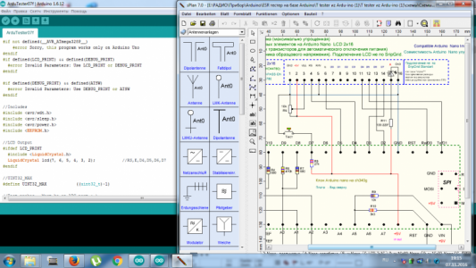
Подскажите пожалуйста, что Вы делали, по возможности подробней, т.к. я совсем в этой теме зеленый. Заранее благодарен. Сергей
всем привет, у меня проблема, загрузил скетчи все которые только тут были, все компилируется но почему то не работает.... горят квадратики слабенько верхний ряд, проверял дисплей и конвертер i2c все работает, SDA и SCLдисплея подключать к А4, А5 или к SDA SCL дуины? перепробовал все варианты не было изменений, может я что-то делаю не так((
у меня проблема, загрузил скетчи все которые только тут были, все компилируется но почему то не работает.... горят квадратики слабенько верхний ряд, проверял дисплей и конвертер i2c все работает,
В скетче из поста 18 раскомментировали нужные строки?
SDA и SCL дисплея подключать к А4, А5 или к SDA SCL дуины?
Для Arduino Uno/Nano/ProMini это равнозначно, а на других Ардуинах (Mega, Leonardo) скетч не проверял.
раскоментил 1602 i2c только одну же строку нужно раскоментить? из-за сопротивлений возможны глюки? когда нажимаю тест кнопку чуток притухает дсплей
не совпадение выводов в скейче со схемой, схему прилагаю
ArduTester07f
Подскажите пожалуйста, что Вы делали, по возможности подробней, т.к. я совсем в этой теме зеленый. Заранее благодарен. Сергей
Вы оказывается скетч ArduTester07f компилируете. Он в моих архивах только для примера приведён, так как автор его 3 года назад забросил. Компиляцию он проходит, но за работоспособность его не ручаюсь.
раскоментил 1602 i2c только одну же строку нужно раскоментить?
В посте 18 написано: Для дисплея LCD 1602 с I2C-интерфейсом комментарий снимается с двух строк: #define LCD1602 и #define LCD_I2C.
А #define NOK5110 нужно закомментировать.
раскоментил 1602 i2c только одну же строку нужно раскоментить?
В посте 18 написано: Для дисплея LCD 1602 с I2C-интерфейсом комментарий снимается с двух строк: #define LCD1602 и #define LCD_I2C.
А #define NOK5110 нужно закомментировать.
#define LCD1602
#define LCD_I2C
//#define NOK5110
вот так выставлено,но эфекта нет(((( у меня дисплей синий , в этом может быть дело?
у меня дисплей синий , в этом может быть дело?
Я так понимаю, что у синего просто подсветка по другому сделана.
А в Serial Monitor скетч что-нибудь выдаёт?
у меня дисплей синий , в этом может быть дело?
Я так понимаю, что у синего просто подсветка по другому сделана.
А в Serial Monitor скетч что-нибудь выдаёт?
TransistorTester
forArduino 1.08a
Ttester 1.08.2
testing...A
2-||-3 Vloss=1.6%
177.7uF ESR=21ohm
щас там стоит 100нан,без него тоже примерно такое же значение показывает
Спасибо за помощь, библиотеки скачал. Буду обращаться к ua6em.
Нужна билиотека I2C, без неё не заработает
щас там стоит 100нан,без него тоже примерно такое же значение показывает
Взял свой скетч из поста 18 (раскомментировал/закомментировал нужное), соединил детальки как описано в постах 2,3,5 и с конденсатором 100 нФ получил следующий результат:
Serial Monitor выдал аналогичное:
TransistorTester
forArduino 1.08a
Ttester 1.08.2
testing...
1-||-3 Vloss=1.0%
109.9nF ESR=16ohm
я не сомневаюсь в работоспособности кода, если я подключу чисто дисплей без всех делителей чтобы проверить чисто дисплей он будет работать? или нужно обязательно все резисторы ставить?
будет!
По дисплею I2C
1. Залить программу определяющую адрес дисплея, смотрим в мониторинге порта
2. В коде инициализации дисплея подставляем этот адрес (скетча)
если я подключу чисто дисплей без всех делителей чтобы проверить чисто дисплей он будет работать? или нужно обязательно все резисторы ставить?
Ниже скетч, который выдаёт адреса для I2C-устройств (I2C_scanner):
#include <Wire.h>

void setup()
{
  Wire.begin();
  Serial.begin(9600);
  I2Cscanner();
}

void loop() {}

void I2Cscanner()
{
  byte error, address;
  int nDevices;

  Serial.println("I2C Scanner");

  nDevices = 0;
  for (address = 1; address < 127; address++)
  {
    Wire.beginTransmission(address);
    error = Wire.endTransmission();

    if (error == 0)
    {
      Serial.print("I2C device found at address 0x");
      if (address < 16)
        Serial.print("0");
      Serial.println(address,HEX);

      nDevices++;
    }
    else if (error == 4)
    {
      Serial.print("Unknow error at address 0x");
      if (address < 16)
        Serial.print("0");
      Serial.println(address,HEX);
    }
  }

  if (nDevices == 0)
    Serial.println("No I2C devices found");
  else {
    Serial.print("Found ");
    Serial.print(nDevices);
    Serial.println(" devices");
  }

  Serial.println();
}
Полученный адрес вставляется в строку 1253 скетча tt108002.ino вместо 0x3F:
LiquidCrystal_I2C lcd(0x3F, 16, 2);
если я подключу чисто дисплей без всех делителей чтобы проверить чисто дисплей он будет работать? или нужно обязательно все резисторы ставить?
Ниже скетч, который выдаёт адреса для I2C-устройств (I2C_scanner):
#include <Wire.h> void setup() { Wire.begin(); Serial.begin(9600); I2Cscanner(); } void loop() {} void I2Cscanner() { byte error, address; int nDevices; Serial.println("I2C Scanner"); nDevices = 0; for (address = 1; address < 127; address++) { Wire.beginTransmission(address); error = Wire.endTransmission(); if (error == 0) { Serial.print("I2C device found at address 0x"); if (address < 16) Serial.print("0"); Serial.println(address,HEX); nDevices++; } else if (error == 4) { Serial.print("Unknow error at address 0x"); if (address < 16) Serial.print("0"); Serial.println(address,HEX); } } if (nDevices == 0) Serial.println("No I2C devices found"); else { Serial.print("Found "); Serial.print(nDevices); Serial.println(" devices"); } Serial.println(); }Полученный адрес вставляется в строку 1253 скетча tt108002.ino вместо 0x3F:
LiquidCrystal_I2C lcd(0x3F, 16, 2);
спасибо, вечером попробую
Р.S. все работает спасибо, но показания всеравно какие то не такие, подключил резистор на 10 кОм он пишет No unknown or damaged part, либо как будто конденсатор на 170vrA? это может быть связано с тем что собрано на макетке беспаячной?
показания всеравно какие то не такие, подключил резистор на 10 кОм он пишет No unknown or damaged part, либо как будто конденсатор на 170vrA? это может быть связано с тем что собрано на макетке беспаячной?
Возможно из-за плохого контакта на беспаечной макетной плате. Ещё светодиод на пине 13 иногда мешает.
Но я недолго с беспаечной макеткой экспериментировал. Как понял, что с 6 резисторами Ардуина может как транзистор-тестер работать, так сразу спаял плату, которую и показал в посте 3.
показания всеравно какие то не такие, подключил резистор на 10 кОм он пишет No unknown or damaged part, либо как будто конденсатор на 170vrA? это может быть связано с тем что собрано на макетке беспаячной?
Возможно из-за плохого контакта на беспаечной макетной плате. Ещё светодиод на пине 13 иногда мешает.
Но я недолго с беспаечной макеткой экспериментировал. Как понял, что с 6 резисторами Ардуина может как транзистор-тестер работать, так сразу спаял плату, которую и показал в посте 3.
))) понял, макетки под рукой нету, придется травить,спасибо за помощь
Интересно, а появится ли когда нибудь прошивка и программа к PC, что бы результаты измерений видеть не на экранчике, а на мониторе (там графичеких возможностей поболе)?
Интересно, а появится ли когда нибудь прошивка и программа к PC, что бы результаты измерений видеть не на экранчике, а на мониторе (там графичеких возможностей поболе)?
Скетчи выдают результаты также и в Serial Monitor, так что желающие могут сделать программу для PC и изображать измерения в любом удобном виде на мониторе.
Спасибо, кто откликнулся на мои просьбы! Схема была собрана на макетке, сегодня разобрал ее и снова собрал аналогично, как в посту 3. Скейч с 1 поста залился, но при включении яркость дисплея и надписи яркие, затем начинают тухнуть и становятся еле видными. Сейчас немного проветрюсь, займусь снова, но прогресс на лицо - это уже радует!!! Как отлажу, выложу фото.
Спасибо, кто откликнулся на мои просьбы! Схема была собрана на макетке, сегодня разобрал ее и снова собрал аналогично, как в посту 3. Скейч с 1 поста залился, но при включении яркость дисплея и надписи яркие, затем начинают тухнуть и становятся еле видными. Сейчас немного проветрюсь, займусь снова, но прогресс на лицо - это уже радует!!! Как отлажу, выложу фото.
если дисплей от нокии то у них помоему у большинства проблема с прилеганием резинок к плате... я такой выкинул так и не смог побороть такую как у тебя проблему
при включении яркость дисплея и надписи яркие, затем начинают тухнуть и становятся еле видными
В библиотеке LiquidCrystal-I2C есть команды для включения/отключения подсветки:
lcd.backlight();
lcd.noBacklight();
не машает ли ему на 13 пине светодиод дуинывский?
Не помню в каких случаях, но светодиод на 13 пине мне мешал, поэтому на Nano я его удалил (точнее удалил резистор к нему - о чём и написал в посте 3).